
Turnkey Analog & Mixed-Signal ASIC Sourcing
Consolidate multi-chip discrete analog front-ends, power regulators, and interface transceivers into a monolithic silicon die. Fast-track 16-week tape-out to engineering samples, achieving 60%–80% BOM reduction with zero single-source supply chain risks.
⚡ Executive Engineering Sourcing Summary (BLUF): Cosine Nanoelectronics provides full-turnkey analog and mixed-signal ASIC design and ODM foundry manufacturing across 0.18µm BCD down to 55nm CMOS nodes with TSMC, SMIC, and Hua Hong. Through systematic discrete BOM consolidation (operational amplifiers, comparators, LDO regulators, reference sources, and interface transceivers), clients achieve a 60% to 80% reduction in total BOM costs, up to 70% PCB area savings, and robust intellectual property anti-reverse-engineering protection within a predictable 16-week workflow from specification freeze to tested engineering samples.
Replacing multiple discrete SMT ICs and passive networks with a single monolithic silicon die.
Continuous schedule from initial discrete BOM audit to packaged, tri-temp tested engineering samples.
BCD & CMOS wafer fabrication with TSMC, SMIC, and Hua Hong for optimal voltage & density.
Proprietary silicon encapsulation and buried traces make competitor reverse engineering virtually impossible.
Why Transition from Discrete SMT to Custom ASIC?
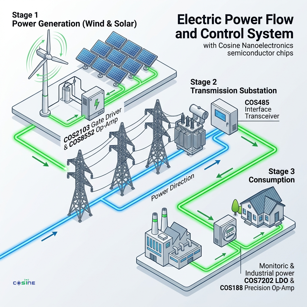
High-volume industrial systems, smart meters, automotive modules, and medical instrumentation often face severe challenges with discrete component architectures: escalating PCB space constraints, assembly yield losses across dozens of SMT placements, and persistent supply chain obsolescence from multiple overseas suppliers.
Cosine's Turnkey ASIC ODM service resolves these roadblocks by merging discrete operational amplifiers, comparators, precision bandgap references, high-voltage LDOs, and interface transceivers into one dedicated silicon chip tailored exactly to your electrical boundaries.
- BOM Consolidation: Reduces component line items from 20+ down to a single orderable part number.
- PCB Miniaturization: Frees up 60%–70% of board footprint, enabling ultra-compact enclosure designs.
- Enhanced Reliability: Drastically fewer solder joints, eliminating cold solder and vibration failure modes.
- IP Secrecy: Proprietary firmware and analog parameters are locked in silicon, preventing unauthorized copying.
Foundry & Packaging Infrastructure
-
✓
Foundry Partnerships: TSMC, SMIC, and Hua Hong. Access to regular MPW shuttle runs and dedicated mask sets.
-
✓
Process Technologies: 0.18µm BCD (high-voltage tolerant up to 40V), 0.11µm eFlash, and 55nm CMOS for digital logic.
-
✓
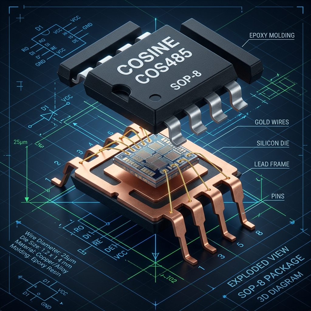
Package Ecosystem: SOP-8/14/16, MSOP-8/10, SOT-23, TSSOP, QFN (2x2mm to 6x6mm), DFN, and Wafer-Level CSP.
-
✓
Wire Bonding: 99.99% pure Gold (Au) wire bonds for automotive/mission-critical reliability, or Copper (Cu) for cost optimization.
-
✓
Quality Qualification: Industrial Grade (-40°C to +85°C/+105°C) and AEC-Q100 Grade 1 (-40°C to +125°C).
-
✓
Flexible Volume: Engineering prototype MPW runs from 50 wafers; production ramp MOQ 100,000 pcs.
The 16-Week Continuous Turnkey ASIC Workflow
From discrete schematic teardown to packaged, production-tested silicon samples in 16 structured weeks.
Phase 1: System Architecture, BOM Audit & Feasibility Assessment
Milestone: SAS Sign-offOur senior analog architects perform a line-by-line audit of your current discrete schematic. We catalog op-amps, comparators, discrete passives, LDO regulators, and interface chips to determine optimal silicon partition boundaries. We calculate target pin counts, evaluate package thermals, and select the target process node (0.18µm BCD or 55nm CMOS).
Phase 2: Analog/Mixed-Signal IP Integration, Schematic Capture & Corner Simulation
Milestone: Schematic FreezeDesigners map functional blocks into Cosine's pre-verified analog silicon IP library (bandgaps, auto-zero chopper stages, low-quiescent LDOs, ±15kV ESD structures). We execute exhaustive SPICE transient and AC simulations across PVT corners (Process: SS/TT/FF, Voltage: ±10%, Temperature: -40°C to +125°C) and run 1,000-point Monte Carlo mismatch simulations to guarantee 6-sigma production yields.
Phase 3: Full-Custom Physical Layout, Parasitic Extraction (PEX) & Tape-Out Prep
Milestone: GDSII Golden Tape-OutPhysical layout engineering using common-centroid symmetrical matching, guard-ring substrate isolation for cross-talk suppression, and wide metal power bussing to minimize electromigration. We execute Parasitic Extraction (PEX) and back-annotated post-layout simulation. Rigorous DRC (Design Rule Check), LVS (Layout Versus Schematic), and ERC checks are validated with foundry rule decks.
Phase 4: Silicon Wafer Fabrication at Tier-1 Foundries (TSMC / SMIC / Hua Hong)
Milestone: Wafer Out VerificationGDSII tooling is released into premier foundry production lines. Wafers undergo photolithography, ion implantation, thin-film chemical vapor deposition, and metallization on 8-inch or 12-inch silicon lines. Inline PCM (Process Control Monitor) electrical testing verifies sheet resistances, threshold voltages, and junction breakdowns against golden foundry specifications.
Phase 5: Automated Packaging, CP Wafer Sort & Tri-Temperature ATE Final Test
Milestone: Engineering Samples DeliveredWafers are probed (Circuit Probing / CP wafer sort) to map bad dies. Good dies undergo precision laser dicing, die attach, 99.99% Au gold wire bonding, and automated transfer molding into specified packages (SOP, MSOP, QFN, DFN). Finished ICs undergo 100% automated test equipment (ATE) Final Testing (FT) across -40°C, +25°C, and +125°C. Samples are mounted onto custom evaluation boards and dispatched via air courier.
16-Week ASIC Execution Milestone Matrix
Clear engineering gates and formal sign-offs ensuring predictable progress and zero specification creep.
Pre-Verified Silicon IP Library
Leverage Cosine's silicon-proven analog IP building blocks to de-risk tape-out and eliminate redundant R&D cycles.
Silicon Architecture & Packaging Verification
Initiate Custom ASIC Consultation & Feasibility Study
Send us your target discrete schematic or system specifications. All inquiries are protected under a mutual Non-Disclosure Agreement (NDA).