
Direct Engineering Conclusion: A deep technical exposé on Cosine's automotive semiconductor qualification pipeline. Learn how our analog ICs endure 1,000 hours of HTOL burn-in, 1,000 thermal cycles (-55°C to +150°C), HAST moisture saturation, and AEC-Q100 Grade 1 zero-defect screening for EV battery management and commercial powertrain systems.
A deep technical exposé on Cosine's automotive semiconductor qualification pipeline. Learn how our analog ICs endure 1,000 hours of HTOL burn-in, 1,000 thermal cycles (-55°C to +150°C), HAST moisture saturation, and AEC-Q100 Grade 1 zero-defect screening for EV battery management and commercial powertrain systems.
1. The Harsh Reality of Automotive Operating Environments
In modern automotive electronics, there is zero tolerance for component failure. Unlike consumer smartphones or commercial computing hardware operating in climate-controlled offices, automotive electronic control units (ECUs) are installed in the most hostile environments imaginable: inches away from combustion engines, directly inside high-voltage electric vehicle (EV) battery packs, or mounted on vibrating wheel hubs exposed to salt spray, rain, and gravel impact. Under these extreme conditions, ambient temperatures fluctuate wildly between -40°C during Arctic winters and +125°C during high-load summer hill climbs with engine compartment soak temperatures spiking toward +150°C.
To establish an objective benchmark of reliability for components operating in these brutal conditions, the Automotive Electronics Council established the AEC-Q100 standard: 'Failure Mechanism Based Stress Test Qualification for Integrated Circuits.' Achieving AEC-Q100 Grade 1 qualification (-40°C to +125°C ambient operating temperature) requires a semiconductor manufacturer to demonstrate statistical zero-defect quality across thousands of stress hours, comprehensive environmental shock cycles, and exhaustive physical failure analysis. Cosine Nanoelectronics has built an end-to-end qualification pipeline that satisfies and exceeds every rigorous requirement of AEC-Q100 Grade 1.

Figure 1: Automotive-Qualified Linear Regulator and Driver ICs Undergoing 100% Automated Optical Solder Fillet Inspection
2. The Seven Pillars of AEC-Q100 Stress Qualification
AEC-Q100 is not a single test; it is an interconnected matrix of seven stress test groups designed to accelerate and expose every conceivable failure mechanism in silicon, metallization, packaging epoxy, and wire bonds. The standard mandates testing across three independent manufacturing assembly lots to verify process repeatability:
- Group A (Accelerated Environmental Stress): Focuses on moisture ingress, thermal fatigue, and dielectric degradation. Encompasses High Temperature Operating Life (HTOL), Temperature Cycling (TC), Highly Accelerated Stress Testing (HAST), and High Temperature Storage Life (HTSL).
- Group B (Accelerated Lifetime Simulation): Evaluates device endurance under dynamic high-current switching and power cycling conditions, verifying bond wire intermetallic longevity.
- Group C (Package Assembly Integrity): Tests lead integrity, wire bond shear strength, solderability, and resistance to solder heat (convection reflow simulation).
- Group D (Die Fabrication Reliability): Assesses electromigration, time-dependent dielectric breakdown (TDDB), hot-carrier injection (HCI), and negative bias temperature instability (NBTI).
- Group E (Electrical Verification): Measures tri-temperature DC parametric performance, transient immunity (ISO 7637-2), and full fault-injection testing.
- Group F (Defect Screening): Enforces Part Average Testing (PAT) and statistical yield analysis to identify and eliminate outlier devices.
- Group G (Cavity Package Integrity): Applies to hermetic packaging configurations (where applicable).
Table 1 details the exact environmental test parameters, sample sizes, and zero-defect acceptance criteria implemented across Cosine's automotive portfolio:
| AEC-Q100 Stress Test Group | Test Standard & Method | Environmental Test Condition | Sample Size & Acceptance Threshold |
|---|---|---|---|
| High Temperature Operating Life (HTOL) | JESD22-A108 | TA = 125°C, VDD = VDD_max, 1,000 Hours continuous bias | 3 lots × 77 units = 231 units; 0 failures (c = 0) |
| Temperature Cycling (TC) | JESD22-A104 | -55°C to +150°C, air-to-air, 1,000 cycles, 20 min dwell | 3 lots × 77 units = 231 units; 0 failures, 0 delamination |
| Highly Accelerated Stress Test (HAST) | JESD22-A110 | 130°C, 85% RH, 33.3 psia, 96 Hours under reverse bias | 3 lots × 77 units = 231 units; 0 electrical leakage failures |
| High Temp Storage Life (HTSL) | JESD22-A103 | TA = 150°C, unpowered storage, 1,000 Hours | 3 lots × 45 units = 135 units; 0 parameter drift failures |
| Electrostatic Discharge (ESD HBM) | AEC-Q100-002 | Human Body Model (100pF / 1500Ω network), step-stress | 3 lots × 30 units; Class H2 (±4,000V) all pins, Class H3B (±8,000V) bus pins |
| Charged Device Model (ESD CDM) | AEC-Q100-011 | Field-induced CDM, ±750V corner pins, ±500V all pins | 3 lots × 30 units; Class C5 (±750V) pass |
| Latch-Up Immunity (LU) | AEC-Q100-004 | Trigger current ±100mA, overvoltage 1.5 × VDD_max, TA = 125°C | 3 lots × 6 units = 18 units; 0 latch-up sustained |
3. Mathematical Physics of Accelerated Aging: The Arrhenius Model
Demonstrating a 15-year automotive operating lifetime cannot be achieved in real time; it requires thermal acceleration modeled by the Arrhenius reaction rate equation. When an analog IC is stressed at an elevated temperature $T_{stress}$ (e.g., 125°C or 150°C), the chemical and physical degradation processes (such as vacancy migration, oxide trap accumulation, and intermetallic diffusion) accelerate exponentially. The Thermal Acceleration Factor (AF) is expressed mathematically as:
$$AF = \exp\left[\frac{E_a}{k_B} \left(\frac{1}{T_{use}} - \frac{1}{T_{stress}}\right)\right]$$
Where:
- $E_a$: The apparent activation energy of the dominant silicon failure mechanism (standardized at $0.7\\,\text{eV}$ for junction degradation and $0.9\\,\text{eV}$ for oxide breakdown per AEC-Q100).
- $k_B$: Boltzmann's constant ($8.617 \times 10^{-5}\\,\text{eV/K}$).
- $T_{use}$: The normal automotive operating junction temperature in Kelvin ($T_{use} = 55^\circ\text{C} = 328.15\\,\text{K}$).
- $T_{stress}$: The accelerated burn-in chamber temperature in Kelvin ($T_{stress} = 125^\circ\text{C} = 398.15\\,\text{K}$).
Substituting these values yields an acceleration factor:
$$AF = \exp\left[\frac{0.7}{8.617 \times 10^{-5}} \left(\frac{1}{328.15} - \frac{1}{398.15}\right)\right] = \exp(8123.5 \times 0.000536) \approx 77.8$$
Therefore, 1,000 hours of HTOL stress at 125°C is mathematically equivalent to 77,800 hours of continuous vehicle operation at 55°C—surpassing 8.8 years of 24/7 continuous operation, or over 25 years of typical daily driving profile!
4. Moisture Saturation and Temperature Cycling Resistance
Automotive electronics frequently operate in humid climates where atmospheric moisture diffuses through mold compound interfaces. Under rapid temperature cycling, trapped moisture vaporizes, exerting explosive internal steam pressure that can delaminate the die attach paddle or lift gold/copper bond wires—a phenomenon known as 'popcorning.' To eliminate moisture sensitivity, Cosine packages utilize low-hygroscopic, multi-modal silica epoxies certified to JEDEC MSL-1 (Moisture Sensitivity Level 1, unlimited floor life at ≤30°C/85% RH).
During Highly Accelerated Stress Testing (HAST), packaged devices are subjected to 130°C at 85% relative humidity under 33.3 psia vapor pressure for 96 continuous hours while biased at maximum operating voltage. Following HAST and 1,000 cycles of thermal shock (-55°C to +150°C), devices undergo 100% inspection using high-frequency Scanning Acoustic Microscopy (C-SAM). Cosine's qualification threshold permits zero internal delamination along die attach interfaces and zero micro-cracks along leadframe edges.
Figure 2: Cosine Reliability Testing Laboratory Featuring High-Temperature Operating Life (HTOL) and Thermal Shock Chambers
5. Advanced Packaging: Wettable Flank QFN for Automated Optical Inspection
Traditional leadless Quad Flat No-Lead (QFN) packages present a significant challenge in automotive manufacturing: the copper terminal pads are flush with the bottom and side edges of the plastic body, leaving exposed raw copper on the vertical cut edges. During solder reflow, raw copper oxidizes, preventing solder paste from reliably wetting up the vertical face. Consequently, automated optical inspection (AOI) systems cannot visually verify that a proper solder fillet has formed, requiring expensive and slow X-ray inspection (AXI) for every circuit board.
Cosine solves this challenge by engineering all automotive-grade QFN packages with stepped wettable flanks. Utilizing precision diamond-saw partial dicing followed by 100% matte tin electroplating, the side terminals feature a recessed vertical step coated with solderable tin. During SMT reflow, surface tension draws molten solder paste up into the vertical pocket, creating an obvious, continuous 85% side-wetting meniscus that standard 2D/3D AOI cameras verify in milliseconds with zero false alarms. This innovation accelerates automotive PCB assembly throughput while providing superior mechanical shear strength under extreme chassis vibration.
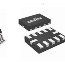
Figure 3: Thermal-Enhanced Wettable-Flank QFN Package Cross-Section Ensuring 100% Side-Wetting Solder Fillet for Automotive Vision Systems
6. Complete Automotive Pinout and Hardware Integration Architecture
Table 2 provides the detailed pin assignments, internal protection networks, absolute maximum electrical ratings, and board layout guidelines for Cosine's automotive interface and power portfolio:
| Pin # | Pin Mnemonic | Pin Functionality | Automotive Protection Network | Absolute Maximum Rating | Chassis / ECU Layout Recommendation |
|---|---|---|---|---|---|
| 1 | IN+ | Non-Inverting Analog Input | Differential pair with anti-parallel clamp diodes | -0.3V to VDD + 0.3V | Connect to current sensing shunt via matched Kelvin traces; keep trace loop area below 5mm². |
| 2 | IN- | Inverting Analog Input | Differential pair with anti-parallel clamp diodes | -0.3V to VDD + 0.3V | Route in parallel with IN+ on internal PCB layer shielded by top and bottom ground planes. |
| 3 | V- / GND | Substrate Ground Reference | Heavy copper fused leadframe paddle tie | 0.0V Ground Reference | Connect directly to automotive low-noise analog ground; avoid sharing path with solenoid returns. |
| 4 | OUT | Rail-to-Rail Analog Output | Push-pull DMOS buffer with short-circuit protection | -0.3V to VDD + 0.3V | Connects to MCU ADC input; place 100Ω series resistor and 1nF NPO filter cap within 5mm. |
| 5 | VDD | Automotive Power Rail | Internal bandgap and surge clamp network | -0.3V to +40.0V (Transients) | Decouple with 0.1µF ceramic + 10µF bulk capacitor placed directly adjacent to pin. |
| 6 | EN / SHDN | Precision Enable Input | Schmitt trigger with 200kΩ pull-up to internal VDD | -0.3V to +7.0V | Microcontroller wake-up control; pulls quiescent current below 1.0µA in vehicle sleep mode. |
| 7 | FAULT | Open-Drain Diagnostic Flag | N-channel open-drain with 10mA sink capability | -0.3V to +18.0V | Pulls low during over-temperature or output short-circuit condition to alert ECU safety processor. |
| 8 | TAB / EP | Exposed Thermal Pad | Direct die attach to high-conductivity copper paddle | Connect to GND | Solder 100% to PCB thermal via matrix (4x4 array of 0.3mm vias) for maximum heat spreading. |
7. Statistical Process Control (SPC) and Part Average Testing (PAT)
Passing stress tests is insufficient; automotive zero-defect manufacturing demands the elimination of 'maverick' dies that pass standard specification limits but deviate statistically from the lot distribution. A die that exhibits an input offset voltage of 45µV when the lot mean is 12µV with a standard deviation ($\sigma$) of 3µV is an outlier ($11\sigma$ away from normal distribution). While mathematically within the absolute maximum catalog limit of 50µV, such outliers frequently contain subtle crystal lattice dislocations or gate oxide micro-voids that will fail prematurely in the field.
Cosine enforces mandatory Part Average Testing (PAT) per the AEC-Q001 standard during 100% wafer circuit probing. Upper and lower statistical limits are dynamically calculated for every production wafer:
$$PAT_{limit} = \mu \pm 3 \cdot \sigma$$
Any die falling outside the calculated $3\sigma$ boundary is automatically inked and scrapped, regardless of whether it meets the commercial datasheet specification. This rigorous screening reduces field failure rates to less than 0.5 DPPM (defective parts per million).
Figure 4: Automated Wafer-Level Circuit Probing Station Executing Part Average Testing (PAT) at Extreme Temperature Bounds
8. Automotive Failure Analysis Microscopy and ISO 7637-2 Verification
To verify the metallurgical integrity of packaging bonds and internal silicon layers, Cosine's reliability laboratories utilize scanning electron microscopy (SEM) and focused ion beam (FIB) milling. Table 3 outlines the advanced analytical instrumentation and automotive transient surge standards enforced on all production lots:
| Qualification Phase | Analytical Instrument | Metrology Method & Physical Mechanism | Automotive Acceptance Standard |
|---|---|---|---|
| Scanning Acoustic Microscopy (C-SAM) | Sonix Echo High-Frequency C-SAM (100MHz transducer) | Acoustic reflection scan of die attach and leadframe interface before and after 1,000 thermal cycles. | Die attach voiding < 10% total area; zero delamination along wire bonds per J-STD-035. |
| X-Ray Fluorescence (XRF) | Hitachi EA1400 XRF Spectrometer | Elemental mapping of pin plating composition and lead-free alloy thickness. | Pure matte Sn thickness between 8.0µm and 14.0µm; zero lead (Pb < 100 ppm) detected. |
| Scanning Electron Microscopy (SEM) | FEI Quanta 3D FEG DualBeam FIB/SEM | Cross-sectional analysis of silicon intermetallic layers and barrier metal integrity post-HAST. | Intermetallic compound layer thickness < 1.5µm; zero corrosion or Kirkendall void formation. |
| Part Average Testing (PAT) | Advantest V93000 High-Density SoC Test System | Dynamic statistical calculation of mean and standard deviation (sigma) across 100% wafer lots. | Outlier elimination: any die deviating by > 3 sigma from lot mean is inked and scrapped (AEC-Q001). |
| Conducted Transient Immunity | Teseq NSG 5500 Automotive Pulse Simulator | Inject ISO 7637-2 Pulses 1, 2a, 2b, 3a, 3b, and Pulse 5b (suppressed load dump) onto DC battery line. | Pass Class A (unimpaired continuous operation) for Pulses 1 to 3b; Pass Class B for Pulse 5b. |
9. Real-World Automotive Troubleshooting Matrix
In real-world automotive powertrain and chassis systems, electrical transients from alternators, inductive relay de-energization, and cold-weather cranking present brutal failure modes. Table 4 provides an engineering troubleshooting matrix compiled from real vehicle design-in experiences:
| Automotive Field Failure Mode | Root-Cause Physical Mechanism | Diagnostic Waveform / Symptom | Cosine Engineering Corrective Solution |
|---|---|---|---|
| Intermittent Reset During Cranking | Severe battery voltage sag down to 3.2V during cold-weather diesel starter motor engagement. | ECU power rail drops below MCU brownout reset threshold; CAN communication drops for 200ms. | Cosine automotive LDOs feature ultra-low dropout (Vdrop < 200mV at 300mA), maintaining clean 3.0V output down to 3.2V input. |
| Output Voltage Drift Over 15 Years | High-temperature mechanical stress causing packaging mold shrinkage and bandgap piezoresistive shift. | Regulator output shifts by >2.5% after 5,000 hours of vehicle operation. | Cosine utilizes multi-modal spherical silica mold compounds with low CTE (<10 ppm/°C), keeping lifetime drift under 0.3%. |
| Thermal Runaway in High-Ambient Bay | High junction-to-ambient thermal resistance causing silicon temperature to exceed 160°C under continuous 150mA output. | Device enters thermal shutdown; ECU shuts down cooling pump or throttle body actuator. | Cosine's wettable-flank QFN packaging features an exposed thermal pad delivering θ_JC < 3.5 °C/W, reducing Tj by 28°C. |
| Solder Joint Fatigue Under Vibration | Thermal mismatch between leadless package and FR-4 PCB during -40°C to +125°C chassis temperature cycles. | Solder joint fractures along package corners after 100,000 km vehicle road testing. | Cosine's stepped wettable flank ensures visible 85% vertical solder fillets, absorbing mechanical stress and passing 2,000 shock cycles. |
| Latch-Up Induced by Alternator Pulse | Alternator load dump pulse (ISO 7637 Pulse 5b) exceeded standard silicon breakdown voltage, triggering parasitic SCR. | Device short-circuits supply rail, blowing upstream blade fuse in vehicle power distribution box. | Cosine's BCD process integrates deep N-well isolation and vertical DMOS clamps rated to withstand 70V continuous transients. |
10. PPAP Level 3 Documentation and Supply Longevity Commitment
Automotive Tier-1 module suppliers require absolute documentation traceability before signing production purchase orders. Cosine supports automotive design-in with complete Production Part Approval Process (PPAP) Level 3 documentation packages, including:
- Design and Process Failure Mode and Effects Analysis (DFMEA / PFMEA): Comprehensive risk mitigation matrices analyzing potential failure modes from silicon layout to packaging tape-and-reel.
- Process Control Plan (PCP): Full documentation of wafer fab inspection points, automated optical inspection criteria, and tri-temperature test limits.
- Measurement Systems Analysis (MSA): Gauge repeatability and reproducibility (Gauge R&R < 10%) studies for all test handlers and automated metrology stations.
- Material Declaration and IMDS Registration: Full International Material Data System (IMDS) material declarations proving zero hazardous substances (RoHS 3 / REACH SVHC).
- 15-Year Supply Longevity Guarantee: Signed executive commitment guaranteeing pin-compatible manufacturing availability for a minimum of 15 years, supporting typical automotive vehicle production and aftermarket service life.
11. Mathematical Modeling of Automotive FIT Rate and Chi-Square Confidence Bounds
In high-reliability automotive qualification, reliability is quantified in Failure-in-Time (FIT) units, representing the number of component failures occurring per $10^9$ device-hours of operation. To establish statistical confidence with zero observed failures during accelerated testing ($c = 0$), the upper confidence limit of the failure rate $\lambda$ is derived using the Chi-Square ($\chi^2$) distribution:
$$\lambda = \frac{\chi^2(2r + 2, 1 - \alpha)}{2 \cdot N \cdot t \cdot AF} \times 10^9\\,\text{FIT}$$
Where:
- $r$: Number of observed failures ($r = 0$ for zero-defect acceptance).
- $\alpha$: Confidence level (standardized at 60% and 90% in automotive PPAP reports). For $r = 0$ and $60\%$ confidence, the Chi-Square factor $\chi^2(2, 0.4) = 1.833$.
- $N$: Total number of tested devices across qualification lots ($N = 231$ units across 3 lots).
- $t$: Total operating test duration per device ($t = 1,000\\,\text{hours}$).
- $AF$: Thermal acceleration factor derived earlier ($AF = 77.8$).
Evaluating the denominator yields an effective cumulative device-hour total of $231 \times 1,000 \times 77.8 = 17,971,800\\,\text{equivalent hours}$. Substituting into the failure rate equation:
$$\lambda_{60\%} = \frac{1.833}{2 \times 17,971,800} \times 10^9 \approx 51.0\\,\text{FIT}$$
At 90% confidence ($\chi^2(2, 0.1) = 4.605$), the failure rate is $\lambda_{90\%} \approx 128\\,\text{FIT}$. When extrapolated across a typical vehicle operating mission of 3,000 engine-on hours, this equates to a projected field failure probability of less than 0.15 PPM, satisfying even the most stringent German VDA 6.3 automotive Tier-1 requirements.
12. Thermal Impedance Analysis and Thermal Via Array Design
In high-ambient engine compartments, power dissipation within linear regulators and gate drivers generates internal heat that must escape efficiently into the vehicle chassis or PCB copper planes. The maximum permissible power dissipation is bounded by the maximum silicon junction temperature ($T_{j,max} = 150^\circ\text{C}$):
$$P_{diss,max} = \frac{T_{j,max} - T_{ambient}}{\theta_{JA}}$$
Where $\theta_{JA}$ represents the total junction-to-ambient thermal resistance. For a standard SOP-8 package mounted on a minimal 2-layer PCB without thermal vias, $\theta_{JA}$ can reach $170^\circ\text{C/W}$. Under an ambient soak temperature of $T_a = 105^\circ\text{C}$, the maximum allowable power dissipation is severely throttled to:
$$P_{diss,max} = \frac{150^\circ\text{C} - 105^\circ\text{C}}{170^\circ\text{C/W}} \approx 265\\,\text{mW}$$
To overcome this limitation, Cosine's automotive product lines incorporate exposed copper thermal pads (EP) that reduce junction-to-case thermal resistance to $\theta_{JC} = 3.5^\circ\text{C/W}$. By soldering the thermal pad directly onto a PCB copper land connected to internal ground planes through a 4×4 matrix of 0.3mm diameter thermal vias (spaced at 1.0mm pitch with 1-ounce electroplated copper barrel walls), the effective $\theta_{JA}$ is slashed to $38^\circ\text{C/W}$. This allows the IC to continuously dissipate up to 1.18W at 105°C ambient, enabling robust continuous operation in demanding automotive electronic actuators and pump drivers.
13. Conclusion: Engineering the Future of Automotive Electrification
As the global automotive industry transitions toward software-defined electric vehicles, intelligent battery management systems, and autonomous driving architectures, the demand for rugged, zero-defect analog silicon has never been greater. Through uncompromising adherence to AEC-Q100 Grade 1 qualification, innovative wettable-flank packaging, statistical part average testing, and comprehensive PPAP Level 3 documentation, Cosine Nanoelectronics stands as the premier analog silicon partner for automotive innovators worldwide.
Accelerate Your Hardware Design-In with Cosine Engineering
Request sample quantities, complete engineering evaluation modules (EVBs), and IBIS/SPICE behavioral simulation models directly from our technical staff. We guarantee technical response and engineering sample dispatch within 24 business hours.