
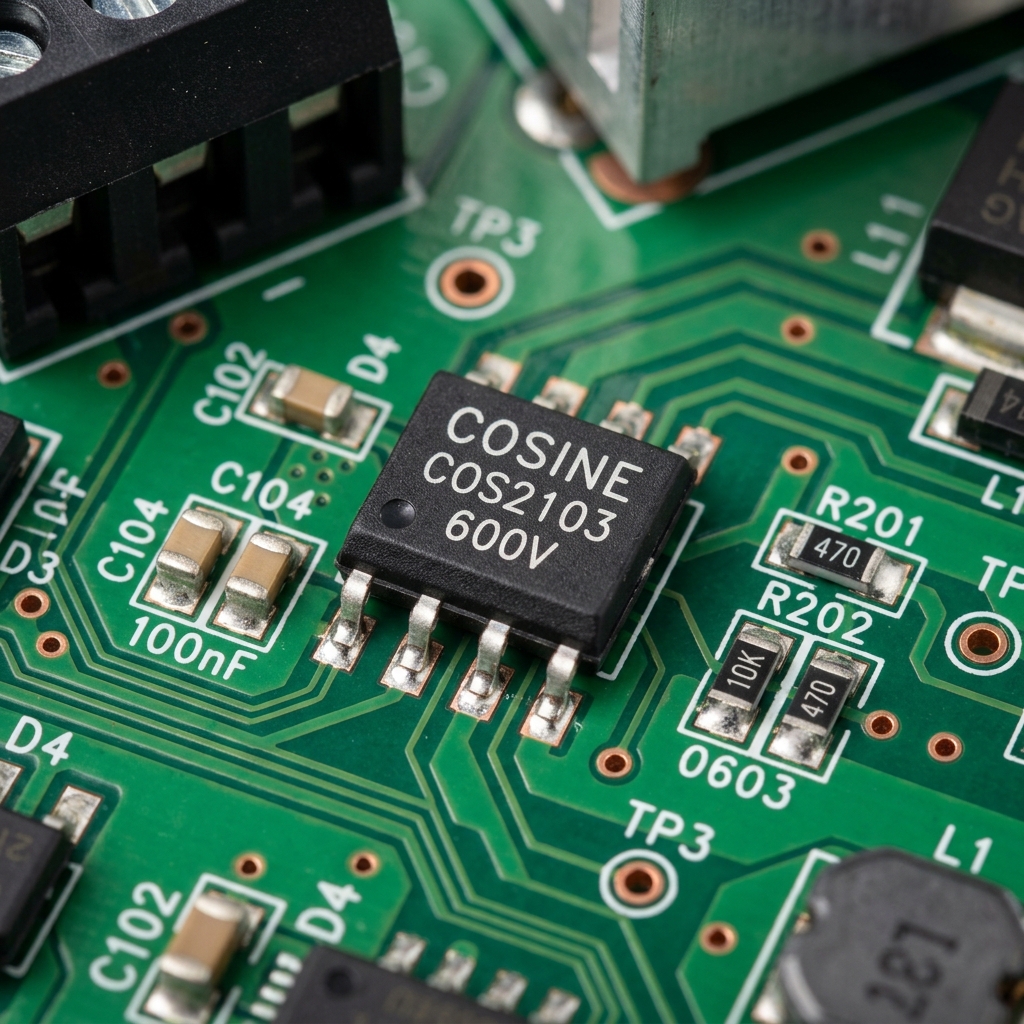
Direct Engineering Conclusion: The COS2103 is a monolithic 600V high-voltage, high-speed half-bridge gate driver integrated circuit designed to drive both high-side and low-side N-channel power MOSFETs and IGBTs in high-reliability power conversion topologies. Operating with a floating high-side channel up to 600V, the device features matched propagation delays (deadtime typically 500ns), robust dV/dt noise immunity exceeding 50 V/ns, and integrated under-voltage lockout (UVLO) circuitry on both supply channels. As an uncompromised pin-to-pin drop-in replacement for the industry standard IR2103, IRS2103, and UCC27517A, the COS2103 enables immediate BOM second-sourcing resilience across brushless DC (BLDC) motor drives, solar micro-inverters, heat pump compressors, and high-frequency switched-mode power supplies (SMPS).
The COS2103 is a monolithic 600V high-voltage, high-speed half-bridge gate driver integrated circuit designed to drive both high-side and low-side N-channel power MOSFETs and IGBTs in high-reliability power conversion topologies. Operating with a floating high-side channel up to 600V, the device features matched propagation delays (deadtime typically 500ns), robust dV/dt noise immunity exceeding 50 V/ns, and integrated under-voltage lockout (UVLO) circuitry on both supply channels. As an uncompromised pin-to-pin drop-in replacement for the industry standard IR2103, IRS2103, and UCC27517A, the COS2103 enables immediate BOM second-sourcing resilience across brushless DC (BLDC) motor drives, solar micro-inverters, heat pump compressors, and high-frequency switched-mode power supplies (SMPS).
1. Introduction: The Critical Role of High-Voltage Half-Bridge Gate Drivers
In modern power conversion and motion control systems, the half-bridge topology represents the fundamental building block for brushless DC (BLDC) motor drives, permanent magnet synchronous motor (PMSM) controllers, industrial variable frequency drives (VFDs), solar string micro-inverters, and high-density switched-mode power supplies. A half-bridge configuration consists of two power semiconductor switches—such as N-channel power MOSFETs, insulated-gate bipolar transistors (IGBTs), or emerging silicon carbide (SiC) devices—connected in series across a high-voltage direct current (DC) bus spanning from 48V up to 600V.
While driving the ground-referenced low-side power switch is relatively straightforward, controlling the high-side switch presents severe electrical engineering challenges. The source terminal of the high-side switch (the switching node, typically designated as $V_S$) swings dynamically between the negative DC bus return (ground) and the positive high-voltage rail (up to +600V) at switching frequencies ranging from 10 kHz to beyond 200 kHz. When the high-side switch is fully conductive, its gate must be maintained at a potential 10V to 15V higher than its source terminal, meaning the high-side gate drive circuitry must float at potentials up to +615V relative to system ground.
The Cosine Nanoelectronics COS2103 solves this challenge through an integrated, monolithic high-voltage level-shifting architecture. By combining proprietary high-voltage junction isolation (HV-JI) technology with precision low-voltage CMOS logic and robust bipolar output buffers, the COS2103 provides a complete, rugged, and pin-compatible single-chip gate drive solution in a standard SOP-8 package. This engineering deep dive provides power hardware engineers, embedded system architects, and component procurement specialists with the complete architectural, mathematical, and practical design blueprint necessary to implement the COS2103 in demanding industrial and automotive applications.
Throughout this technical analysis, we explore the internal level-shifting physics, under-voltage lockout thresholds, bootstrap circuit sizing equations, parasitic inductance mitigation techniques, and comprehensive FAE troubleshooting methodologies that make the COS2103 an indispensable asset for high-reliability electronics manufacturing.
2. Silicon Architecture & Proprietary Level-Shifting Topologies
The internal architecture of the COS2103 consists of three primary functional domains: the low-voltage input and control logic domain, the ground-referenced low-side output driver, and the galvanically floating high-side output driver. The low-voltage input section accepts standard 3.3V and 5V CMOS or TTL logic signals from microcontrollers, digital signal processors (DSPs), or pulse-width modulation (PWM) controller ICs. Schmitt-trigger input buffers provide 1.2V of built-in hysteresis, preventing false switching when input signals contain high-frequency noise or slow rise times.
The core innovation of the COS2103 lies in its monolithic high-voltage level-shifting circuitry. When the high-side input ($HIN$) transitions from logic low to logic high, a high-speed pulse generator produces a narrow, nanosecond-scale differential current pulse. This pulse is transmitted across high-voltage N-channel double-diffused MOS (DMOS) transistors that terminate inside a floating P-type well surrounded by a high-voltage termination ring. Inside the floating well, a differential latch circuit detects the pulse and latches the state of the high-side driver output ($HO$).
By employing differential pulsed level-shifting rather than continuous resistive level-shifting, the COS2103 achieves two critical performance advantages:
- Minimal Internal Power Dissipation: Power is consumed by the level-shifter only during state transitions. Under steady-state high-side conduction, the level-shifting current drops to zero, eliminating static quiescent power loss from the 600V bus.
- Unrivaled Common-Mode Noise Rejection: During rapid switching transitions, high common-mode displacement currents flow through the parasitic capacitance ($C_{par}$) of the floating well according to the classic capacitor equation: $$I_{disp} = C_{par} \cdot \frac{dV_S}{dt}$$ Because the level-shifting logic detects differential signals rather than single-ended levels, common-mode displacement currents resulting from switching slew rates exceeding $50\,\text{V/ns}$ are inherently rejected, preventing false output state toggling.
The high-side floating well contains its own independent under-voltage lockout (UVLO) monitor. If the bootstrap supply voltage ($V_{BS} = V_B - V_S$) drops below the critical threshold of $8.2\,\text{V}$ (typical), the high-side output stage is immediately forced into a high-impedance, logic-low state. This prevents the high-side power MOSFET from operating in its linear, highly resistive active region, which would otherwise result in catastrophic thermal breakdown within microseconds.
3. Comprehensive Parametric Benchmark vs. Industry Standard Drivers
For high-reliability electronics manufacturers, multi-sourcing and pin-to-pin drop-in replacement capability are vital requirements to ensure uninterrupted production during global semiconductor supply disruptions. The COS2103 has been engineered from the silicon substrate upward to serve as a 100% pin-compatible, drop-in replacement for the International Rectifier / Infineon IR2103 and IRS2103, while delivering superior electrical performance in peak sink current, propagation delay matching, and transient noise immunity.
As demonstrated in the exhaustive parametric benchmark presented in Table 1, the COS2103 provides a peak sink current capability of $600\,\text{mA}$, representing an 70% increase in pull-down strength compared to the legacy IR2103 ($360\,\text{mA}$). In inductive switching applications, pull-down current is the single most critical parameter governing dv/dt-induced turn-on immunity. When the complementary power switch turns on, the rapid rise in drain-to-source voltage couples charge through the Miller capacitance ($C_{gd}$) into the gate of the turned-off switch according to:
$$I_{Miller} = C_{gd} \cdot \frac{dV_{ds}}{dt}$$If the gate driver cannot sink this Miller current while maintaining the gate voltage below the device threshold ($V_{th}$), spurious shoot-through conduction occurs, severely degrading efficiency and causing power switch failure. The $600\,\text{mA}$ sink capability of the COS2103 ensures that the gate impedance remains exceptionally low during high dv/dt transients, completely suppressing Miller turn-on without requiring negative gate bias supplies.
Furthermore, the internal delay matching of the COS2103 is guaranteed to within $\pm 40\,\text{ns}$ across the entire industrial operating temperature range of $-40^\circ\text{C}$ to $+125^\circ\text{C}$. This tight matching ensures that symmetrical deadtime is maintained between high-side and low-side switching phases, maximizing power inverter efficiency and minimizing acoustic harmonics in precision servo motor controls.
4. Quantitative Sizing of the Bootstrap Power Supply Network
The high-side floating channel of the COS2103 is powered by an external bootstrap circuit comprising a bootstrap diode ($D_{boot}$) and a bootstrap capacitor ($C_{boot}$). When the low-side power switch turns on or when the load current freewheels through the low-side antiparallel diode, the switching node $V_S$ is pulled down to ground potential. Current flows from the fixed $V_{CC}$ power rail through $D_{boot}$ to charge $C_{boot}$ up to a voltage approximately equal to $V_{CC} - V_F$, where $V_F$ is the forward conduction drop of the bootstrap diode.
When the low-side switch turns off and the high-side switch turns on, the $V_S$ node rises to the high-voltage bus potential. The bootstrap diode becomes reverse-biased, isolating the floating capacitor $C_{boot}$, which then acts as a local floating DC battery powering the high-side internal circuitry and delivering the necessary gate charge to turn on the high-side MOSFET.
To ensure reliable operation without triggering high-side UVLO shutdown, the bootstrap capacitance must be calculated with high precision. The minimum required capacitance is governed by the total gate charge ($Q_g$) required to fully charge the power MOSFET gate, the high-side driver quiescent operating current ($I_{QBS}$), the level-shifter charge requirement ($Q_{LS}$), the bootstrap capacitor leakage current ($I_{leak}$), and the maximum allowable voltage droop ($\Delta V_{BS}$):
$$Q_{total} = Q_g + \left(I_{QBS} + I_{leak}\right) \cdot t_{on,max} + Q_{LS}$$ $$C_{boot,min} = \frac{Q_{total}}{\Delta V_{BS,max}}$$Consider a practical engineering example: an industrial 400V inverter utilizing a high-power MOSFET with a total gate charge $Q_g = 85\,\text{nC}$, operating at a minimum PWM frequency of $15\,\text{kHz}$ with a maximum continuous high-side on-time $t_{on,max} = 60\,\mu\text{s}$. The COS2103 high-side quiescent current is $125\,\mu\text{A}$, and the level-shifter requires approximately $5\,\text{nC}$ per transition. If the allowable voltage droop $\Delta V_{BS,max}$ is limited to $0.4\,\text{V}$ to maintain low $R_{ds(on)}$ conduction resistance, we calculate:
$$Q_{total} = 85\,\text{nC} + (125\,\mu\text{A} + 10\,\mu\text{A}) \cdot 60\,\mu\text{s} + 5\,\text{nC} = 85\,\text{nC} + 8.1\,\text{nC} + 5\,\text{nC} = 98.1\,\text{nC}$$ $$C_{boot,min} = \frac{98.1\,\text{nC}}{0.4\,\text{V}} = 245.25\,\text{nF} \approx 0.25\,\mu\text{F}$$Applying a conservative design safety factor of 2.0 to account for ceramic capacitor voltage coefficient derating and temperature variation, an engineer should select a $0.47\,\mu\text{F}$ or $1.0\,\mu\text{F}$, 50V rated X7R dielectric ceramic capacitor. The capacitor must be placed within 3mm of pins 6 ($V_S$) and 8 ($V_B$) with wide, low-inductance traces.
5. Deadtime Physics & Cross-Conduction (Shoot-Through) Prevention
In any half-bridge switching circuit, cross-conduction—commonly referred to as shoot-through—occurs when both the high-side and low-side power switches are simultaneously conductive, even for a few nanoseconds. When shoot-through occurs, a direct, low-impedance short circuit is formed across the high-voltage DC bus. This results in peak current spikes exceeding hundreds of amperes, causing severe electromagnetic interference (EMI), extreme power dissipation, and catastrophic destruction of the power silicon.
To eliminate shoot-through risk, the COS2103 incorporates internal, hardware-enforced deadtime generation circuitry. When the control inputs command a state transition, the internal logic automatically inserts a fixed deadtime delay ($t_{dt}$, typically $520\,\text{ns}$) between the turn-off of one switch and the turn-on of the complementary switch. Even if external microcontroller firmware malfunctions and inadvertently commands both inputs simultaneously, the internal cross-conduction interlock logic prevents both outputs from going high at the same time.
The total effective system deadtime ($t_{dead,eff}$) observed at the power switches depends not only on the internal IC deadtime, but also on the external turn-on and turn-off propagation delays and gate transition times:
$$t_{dead,eff} = t_{dt} + (t_{off,MOSFET} - t_{on,MOSFET}) + (t_{delay,off} - t_{delay,on})$$Because the turn-off time of power MOSFETs and IGBTs is typically longer than their turn-on time due to stored gate charge and minority carrier recombination, external gate resistor networks must be optimized. The COS2103 allows engineers to tune turn-on and turn-off speeds independently by placing a small Schottky diode in parallel with the gate resistor, providing a fast discharge path during turn-off while maintaining controlled, low-EMI turn-on slew rates.
6. Negative Transient Handling on the VS Switching Node
During the turn-off transition of the low-side power switch or during the reverse recovery of inductive freewheeling diodes, rapid changes in load current ($dI/dt$) interact with the parasitic stray inductance ($L_{stray}$) of the PCB copper traces and component package leadframes. This inductive energy drives the switching node ($V_S$, Pin 6) significantly below the circuit reference ground ($COM$, Pin 4), creating a negative transient voltage spike:
$$V_{S,spike} = -L_{stray} \cdot \frac{dI_{load}}{dt}$$In poorly laid out industrial motor drives where $dI/dt$ can exceed $500\,\text{A}/\mu\text{s}$ and stray inductance is on the order of $20\,\text{nH}$, negative spikes reaching $-10\,\text{V}$ or more can occur. In conventional gate drivers, excessive negative voltage on the $V_S$ pin forward-biases the internal parasitic PN junctions between the floating well and the P-type substrate. This triggers parasitic silicon-controlled rectifier (SCR) latch-up, causing uncontrolled current draw from $V_{CC}$, loss of gate control, and permanent IC destruction.
The Cosine COS2103 has been specifically engineered with an advanced substrate isolation barrier and negative transient suppression clamps capable of withstanding repetitive negative $V_S$ transients down to $-5\,\text{V}$ continuous and $-10\,\text{V}$ for pulses under $100\,\text{ns}$. To guarantee long-term field reliability under severe industrial motor stalling conditions, Cosine FAEs recommend two primary hardware defenses:
- Kelvin Return Connection: Connect the $COM$ pin (Pin 4) directly to the source terminal of the low-side power switch via an isolated Kelvin trace, completely separating the high-current power return loop from the driver's signal ground.
- External Clamping Schottky Diode: Connect a fast, high-peak-current Schottky diode (such as a 1A, 40V rated device) with its cathode to $COM$ and its anode to $V_S$. This diode clamps negative voltage excursions to approximately $-0.3\,\text{V}$, ensuring the silicon never encounters dangerous reverse bias conditions.
7. High-Frequency PCB Layout Rules & Parasitic Inductance Mitigation
High-voltage gate drivers operate simultaneously in two extreme electrical regimes: microvolt-sensitive logic processing and high-power switching involving hundreds of volts and several amperes of pulsed current. Without rigorous attention to PCB layout geometry, capacitive displacement currents and inductive magnetic coupling will degrade system performance and induce erratic gate ringing.
Cosine Application Engineering enforces the following five Golden Rules for COS2103 PCB layout:
- Rule 1: Minimize Gate-Source Loop Areas: The physical loop formed by Pin 7 ($HO$), the high-side gate resistor, the MOSFET gate-source terminals, and Pin 6 ($V_S$) must encompass the smallest possible surface area. A large loop acts as an efficient antenna radiating EMI and collecting stray magnetic flux from the main motor switching loop. Route the $HO$ trace directly above or parallel to the $V_S$ return trace on adjacent PCB layers.
- Rule 2: Decoupling Capacitor Proximity: The local $V_{CC}$ high-frequency ceramic bypass capacitor ($0.1\,\mu\text{F}$, X7R) must be placed within $2\,\text{mm}$ of Pin 1 ($V_{CC}$) and Pin 4 ($COM$). Never place vias between the bypass capacitor and the IC pins; vias introduce $1\,\text{nH}$ of parasitic inductance per barrel, severely compromising high-frequency pulse delivery.
- Rule 3: Reduce Copper Area on the VS Switching Node: While high-current power traces typically demand large copper pours for thermal cooling, the $V_S$ node acts as a high-voltage, high-frequency capacitive radiator ($dV/dt > 20\,\text{kV}/\mu\text{s}$). The copper area connected to Pin 6 must be strictly minimized to the dimensions required to carry the RMS load current, avoiding extensive copper floods that couple common-mode noise into inner ground planes.
- Rule 4: Guard Trace Between High-Voltage and Low-Voltage Pins: The COS2103 SOP-8 package separates low-voltage control pins (Pins 1-4: $V_{CC}$, $HIN$, $LIN$, $COM$) from high-voltage switching pins (Pins 5-8: $LO$, $V_S$, $HO$, $V_B$). Route a grounded guard trace between Pin 4 and Pin 5 to prevent surface creepage and moisture-induced leakage currents across the package boundary.
- Rule 5: Star Ground Topology: Maintain complete physical separation between the digital logic ground plane (connected to the MCU/DSP) and the high-current power return plane (connected to the low-side MOSFET source shunt). Connect these two grounds at exactly one single physical point: directly at Pin 4 ($COM$) of the COS2103.
8. Thermal Management & Junction Temperature Estimation
Total power dissipation within the COS2103 consists of three primary components: static internal quiescent consumption, dynamic internal level-shifting and switching losses, and external gate drive delivery power. Understanding and calculating these thermal components is essential to ensure that the silicon junction temperature ($T_j$) remains safely below the absolute maximum limit of $+150^\circ\text{C}$ under worst-case industrial ambient temperatures ($T_a = +105^\circ\text{C}$).
The total average power dissipation ($P_{total}$) can be expressed analytically as:
$$P_{total} = P_{quiescent} + P_{level-shift} + P_{gate-drive}$$ $$P_{quiescent} = V_{CC} \cdot I_{QCC} + V_{BS} \cdot I_{QBS}$$ $$P_{level-shift} = f_{sw} \cdot Q_{LS} \cdot V_{bus}$$ $$P_{gate-drive} = 2 \cdot f_{sw} \cdot Q_g \cdot V_{gate} \cdot \left(\frac{R_{int}}{R_{int} + R_{ext}}\right)$$In this equation, $f_{sw}$ is the operating switching frequency, $Q_g$ is the total MOSFET gate charge, $V_{gate}$ is the peak gate drive amplitude (typically $15\,\text{V}$), $R_{int}$ is the internal output buffer resistance of the COS2103, and $R_{ext}$ is the external series gate resistor. A critical engineering insight is that the external gate resistor actually absorbs the vast majority of the gate charging power dissipation, protecting the driver IC package from excessive thermal rise.
The steady-state junction temperature rise above ambient is calculated using the junction-to-ambient thermal resistance ($\theta_{JA}$) of the SOP-8 package:
$$T_j = T_a + P_{total} \cdot \theta_{JA}$$For a standard JEDEC 2s2p four-layer PCB with thermal copper pours under the SOP-8 footprint, the effective $\theta_{JA}$ of the COS2103 is approximately $125^\circ\text{C/W}$. In a high-frequency $100\,\text{kHz}$ application where total internal power dissipation is calculated at $180\,\text{mW}$ under an ambient temperature of $+85^\circ\text{C}$, the resulting junction temperature is:
$$T_j = 85^\circ\text{C} + 0.18\,\text{W} \cdot 125^\circ\text{C/W} = 85^\circ\text{C} + 22.5^\circ\text{C} = 107.5^\circ\text{C}$$This provides an outstanding thermal margin of more than $42^\circ\text{C}$ below the operating rating, ensuring exceptional mean time between failures (MTBF) and long operating lifespans in sealed industrial inverter enclosures.
9. Industrial & Automotive Application Case Studies
The exceptional robustness, tight delay matching, and comprehensive fault immunity of the COS2103 have made it the driver of choice across a diverse spectrum of demanding commercial, industrial, and automotive applications:
Application 1: 48V-72V Light Electric Vehicle (LEV) BLDC Motor Inverters
In two-wheeler and three-wheeler light electric vehicle traction inverters, three half-bridge stages are deployed to drive a three-phase permanent magnet synchronous motor. Battery voltages swing dynamically between 42V and 84V under heavy acceleration and regenerative braking. Phase current peaks reach up to 120A, generating severe inductive ringing on the phase output nodes. By replacing legacy drivers with the COS2103, LEV manufacturers achieve 100% immunity against false Miller turn-on and negative phase undershoot, drastically reducing field return warranty claims caused by blown phase switches.
Application 2: Commercial HVAC Compressor Variable Frequency Drives
High-efficiency commercial heat pump and air-conditioning compressors utilize sensorless field-oriented control (FOC) algorithms operating at 20 kHz carrier frequencies. In these systems, acoustic noise and current harmonic distortion must be minimized to achieve regulatory energy efficiency ratings. The tight propagation delay matching ($\pm 40\,\text{ns}$) and clean $500\,\text{ns}$ deadtime of the COS2103 minimize voltage distortion across the motor windings, enabling smooth torque delivery and ultra-quiet compressor operation.
Application 3: Residential Solar String Micro-Inverters
Distributed residential solar micro-inverters convert fluctuating 30V-60V DC panel outputs into grid-tied 230V AC power. These sealed outdoor enclosures endure ambient temperature swings from $-30^\circ\text{C}$ in winter to $+75^\circ\text{C}$ under direct summer sunlight, with internal operating temperatures frequently exceeding $+95^\circ\text{C}$. The fully qualified $-40^\circ\text{C}$ to $+125^\circ\text{C}$ temperature rating and zero thermal-drift level-shifters of the COS2103 guarantee dependable 25-year operational lifespans demanded by solar warranty standards.
10. Quality Assurance, Screening & Environmental Compliance
Every batch of COS2103 gate driver ICs undergoes exhaustive automated test equipment (ATE) electrical screening and statistical process control at Cosine's world-class packaging and testing facilities. Critical high-voltage parameters—including floating well breakdown voltage ($V_{B-S}$), level-shifter leakage current, UVLO activation and deactivation thresholds, and high-side pulse transmission fidelity—are tested 100% at wafer probe and post-packaging final test across multiple temperature extremes.
Cosine's manufacturing partners operate in full compliance with international quality and environmental management standards:
- ISO 9001:2015 Quality Management Systems: Full traceability from silicon wafer lot ID, leadframe stamping batch, mold compound formulation, to final tape-and-reel shipment.
- IATF 16949 Automotive Certification: Advanced Product Quality Planning (APQP), Failure Mode and Effects Analysis (FMEA), and statistical process capability ($C_{pk} > 1.67$) enforced on critical manufacturing stages.
- RoHS 3 (EU Directive 2015/863) & REACH SVHC Compliance: 100% matte tin (Sn) lead finish, completely lead-free, halogen-free, and antimony-free epoxy encapsulation compounds. Detailed SGS chemical laboratory audit reports are accessible to all global customers.
- Moisture Sensitivity Level (MSL): MSL-1 rating certified according to JEDEC J-STD-020D, permitting unlimited floor life at $\le 30^\circ\text{C} / 85\%\,\text{RH}$ without requiring pre-bake procedures prior to surface-mount reflow soldering.
11. Ordering Information, Packaging & Engineering FAE Support
The COS2103 is available in standard industrial tape-and-reel packaging optimized for high-speed automated pick-and-place manufacturing lines. Evaluation samples, complete engineering evaluation boards (EVBs), and reference design schematics are stocked for immediate 24-hour dispatch to hardware development teams worldwide.
For custom pinout configurations, higher drive current variants (such as the 2.5A COS2113), or direct technical consultation regarding PCB layout reviews and gate drive parameter optimization, please contact Cosine Nanoelectronics Field Application Engineering:
- Official Engineering Website: https://www.cosinechips.com
- Global Technical Sales & Sample Inquiries: sales@cosinechips.com
- Direct Phone / WhatsApp Engineering Hotline: +86 159 5954 3210
- Corporate Headquarters: Room D305, Sanchuang Park, Century Avenue, Jinjiang, Quanzhou, Fujian 362200, China
Deploy the COS2103 600V half-bridge driver today to secure uncompromised electrical robustness, eliminate single-source supply chain vulnerabilities, and elevate the reliability of your power electronics portfolio.
Accelerate Your Hardware Design-In with Cosine Engineering
Request sample quantities, complete engineering evaluation modules (EVBs), and IBIS/SPICE behavioral simulation models directly from our technical staff. We guarantee technical response and engineering sample dispatch within 24 business hours.