
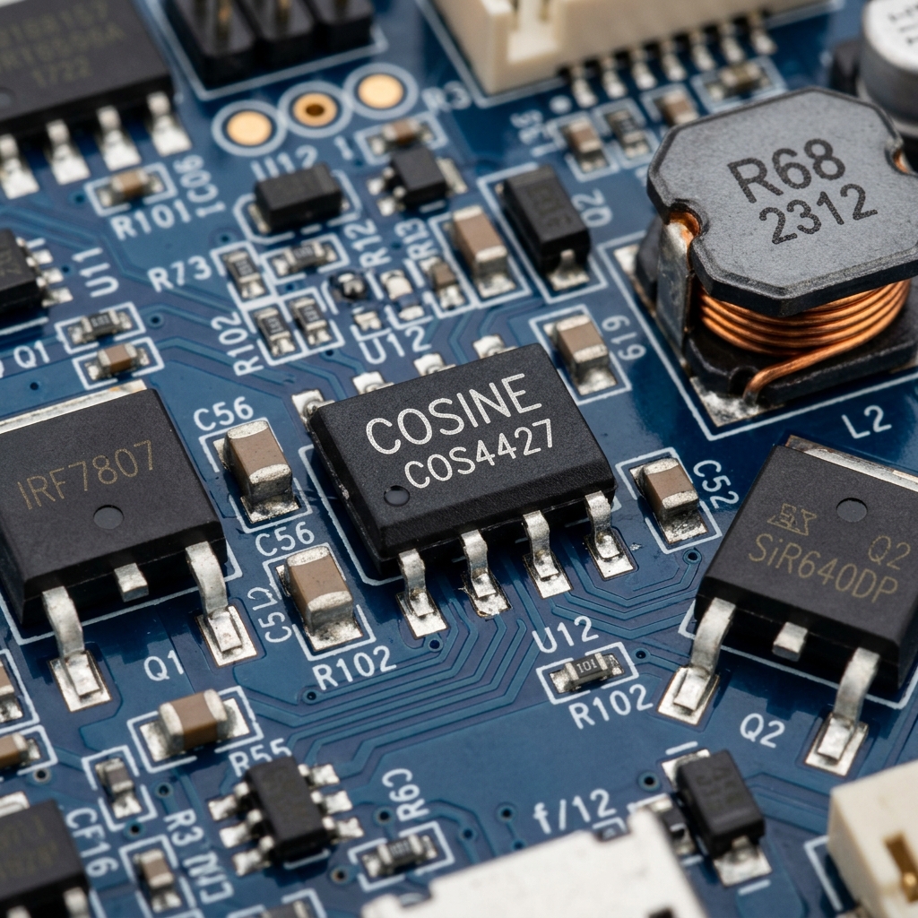
Direct Engineering Conclusion: The COS4427 is a dual-channel non-inverting high-speed low-side power MOSFET and IGBT gate driver capable of delivering 1.5A peak sink and source currents with matched propagation delays under 40ns. Designed to operate across a wide supply voltage range of 4.5V to 18V, the device combines low-power CMOS input buffers directly compatible with 3.3V and 5V microcontrollers with robust bipolar output totem-pole stages. Built-in internal latch-up immunity exceeding 500mA and reverse voltage protection against negative inductive swings down to -5V make the COS4427 the definitive pin-to-pin drop-in replacement for the Microchip TC4427, Maxim MAX4427, and Texas Instruments UCC27524. It is widely implemented across synchronous buck converters, LLC resonant half-bridges, secondary synchronous rectifiers, and high-frequency pulsed laser drivers.
The COS4427 is a dual-channel non-inverting high-speed low-side power MOSFET and IGBT gate driver capable of delivering 1.5A peak sink and source currents with matched propagation delays under 40ns. Designed to operate across a wide supply voltage range of 4.5V to 18V, the device combines low-power CMOS input buffers directly compatible with 3.3V and 5V microcontrollers with robust bipolar output totem-pole stages. Built-in internal latch-up immunity exceeding 500mA and reverse voltage protection against negative inductive swings down to -5V make the COS4427 the definitive pin-to-pin drop-in replacement for the Microchip TC4427, Maxim MAX4427, and Texas Instruments UCC27524. It is widely implemented across synchronous buck converters, LLC resonant half-bridges, secondary synchronous rectifiers, and high-frequency pulsed laser drivers.
1. Introduction: Driving Power MOSFETs and IGBTs at Modern Switching Frequencies
In high-efficiency power electronics, the transition speed of power semiconductor switches dictates system efficiency, power density, and thermal overhead. While modern microcontrollers and digital signal processors (DSPs) provide sophisticated pulse-width modulation (PWM) engines capable of sub-microsecond timing precision, their general-purpose input/output (GPIO) pins are fundamentally limited in output current delivery, typically restricted to 4mA to 20mA at 3.3V or 5V logic levels.
Power MOSFETs and insulated-gate bipolar transistors (IGBTs) are voltage-controlled devices with substantial input capacitances ($C_{iss} = C_{gs} + C_{gd}$). Turning a power MOSFET on or off requires rapidly transferring electrical charge into and out of this input capacitance. If a low-current microcontroller pin attempts to directly drive a power switch, the charging time is extended over hundreds of nanoseconds or even microseconds. During this extended switching interval, the device operates simultaneously under high drain-to-source voltage ($V_{ds}$) and high drain current ($I_d$), resulting in severe instantaneous power dissipation ($P = V_{ds} \cdot I_d$) that rapidly triggers thermal failure.
The Cosine Nanoelectronics COS4427 acts as a dedicated, high-current intermediate power amplifier. By accepting standard low-voltage logic inputs and delivering up to 1.5A of peak pulse current at supply rails up to 18V, the COS4427 charges and discharges power gate capacitances in under 20 nanoseconds. This sharp transition confines switching losses to negligible proportions, enabling system designers to increase PWM carrier frequencies up to 500 kHz and significantly shrink the physical size of inductors, transformers, and output filter capacitors.
2. Architectural Deep Dive: Internal Silicon Topologies and Latch-Up Ruggedness
The internal architecture of the COS4427 comprises two independent, non-inverting driver channels fabricated on a robust high-voltage sub-micron CMOS process. Each channel incorporates a high-speed Schmitt-trigger input buffer, an internal voltage level-translator, an active deadtime and non-overlap logic controller, and a high-current bipolar-CMOS composite totem-pole output stage.
The input stage features wide-range logic threshold detectors engineered with 1.0V of hysteresis. The logic-high threshold ($V_{IH}$) is guaranteed at $2.4\,\text{V}$ maximum, while the logic-low threshold ($V_{IL}$) is set at $0.8\,\text{V}$ minimum across the full operating supply voltage range of $4.5\,\text{V}$ to $18\,\text{V}$. This wide input tolerance allows hardware designers to interface the COS4427 directly with $3.3\,\text{V}$ low-power microcontrollers, $5\,\text{V}$ industrial PLCs, or high-voltage open-collector comparators without requiring external level-shifting buffers or pull-up voltage translators.
The output stage utilizes a parallel combination of high-speed N-channel and P-channel MOSFETs backed by high-current vertical NPN/PNP bipolar transistors. This composite architecture delivers exceptional peak sourcing and sinking capability ($1.5\,\text{A}$) while maintaining an output saturation voltage of less than $0.5\,\text{V}$ to the supply rails during steady-state conduction. Furthermore, proprietary substrate guard rings and deep N-well isolation provide latch-up immunity exceeding $500\,\text{mA}$ of reverse injection current, completely preventing parasitic SCR firing commonly encountered when driving inductive loads.
3. Analytical Sizing of Gate Resistors and Peak Drive Currents
The selection of the external series gate resistor ($R_{gate}$) represents a critical engineering compromise between switching speed and electromagnetic emissions. The peak instantaneous gate current ($I_{peak}$) delivered by the COS4427 is determined by the supply voltage ($V_{DD}$), the internal driver output resistance ($R_{int}$), and the external resistor value:
$$I_{peak} = \frac{V_{DD}}{R_{int} + R_{gate}}$$For the COS4427 operating at $V_{DD} = 12\,\text{V}$ with an internal output resistance $R_{int} \approx 3.5\,\Omega$, selecting an external gate resistor $R_{gate} = 6.8\,\Omega$ yields a controlled peak current of:
$$I_{peak} = \frac{12\,\text{V}}{3.5\,\Omega + 6.8\,\Omega} = \frac{12\,\text{V}}{10.3\,\Omega} \approx 1.165\,\text{A}$$This peak current operates well within the 1.5A rating of the device, protecting the silicon leadframe from excessive bond wire stress while delivering ultra-fast gate charging. The effective turn-on rise time ($t_r$) for a load capacitance $C_{load} = 2200\,\text{pF}$ is calculated from the circuit time constant ($\tau = (R_{int} + R_{gate}) \cdot C_{load}$):
$$t_r \approx 2.2 \cdot \tau = 2.2 \cdot (10.3\,\Omega) \cdot (2200 \times 10^{-12}\,\text{F}) \approx 49.8\,\text{ns}$$In applications where turn-off must be accelerated to prevent shoot-through without altering turn-on slew rate, an anti-parallel fast recovery diode (such as a 1N4148 or BAT54 Schottky) placed across $R_{gate}$ provides an asymmetrical gate resistance, pulling the gate down through a lower impedance during turn-off.
4. Thermal Budgeting and Power Dissipation Mechanics
Operating high-capacitance loads at high PWM frequencies generates dynamic power dissipation within the gate drive subsystem. Total power consumption ($P_{total}$) consists of the static quiescent dissipation ($P_q$) and the dynamic capacitive charging dissipation ($P_{dyn}$):
$$P_{total} = P_q + P_{dyn}$$ $$P_q = V_{DD} \cdot I_{DD}$$ $$P_{dyn} = 2 \cdot C_{load} \cdot V_{DD}^2 \cdot f_{sw}$$A crucial physical principle in gate drive engineering is that the dynamic energy required to charge and discharge the capacitive gate ($E = C_{load} \cdot V_{DD}^2$) is divided between the internal driver resistance ($R_{int}$) and the external gate resistor ($R_{gate}$) in exact proportion to their resistances:
$$P_{IC,int} = P_{dyn} \cdot \left(\frac{R_{int}}{R_{int} + R_{gate}}\right) + P_q$$Consider a dual-channel synchronous rectifier operating at $f_{sw} = 250\,\text{kHz}$ with $V_{DD} = 12\,\text{V}$ and each MOSFET presenting $C_{load} = 1500\,\text{pF}$. The total dynamic power is:
$$P_{dyn} = 2 \cdot (1500 \times 10^{-12}\,\text{F}) \cdot (12\,\text{V})^2 \cdot (250 \times 10^3\,\text{Hz}) = 0.108\,\text{W} = 108\,\text{mW}$$With $R_{int} = 3.5\,\Omega$ and $R_{gate} = 10\,\Omega$, the internal dissipation in the COS4427 silicon is only:
$$P_{IC,int} = 108\,\text{mW} \cdot \left(\frac{3.5\,\Omega}{3.5\,\Omega + 10\,\Omega}\right) + (12\,\text{V} \cdot 1.5\,\text{mA}) = 28.0\,\text{mW} + 18.0\,\text{mW} = 46.0\,\text{mW}$$In the standard SOP-8 package ($\theta_{JA} = 130^\circ\text{C/W}$), this corresponds to an internal junction temperature rise ($\Delta T_j$) of merely $5.98^\circ\text{C}$ above ambient, proving that the COS4427 maintains cool, highly reliable performance even in tightly sealed power supplies.
5. Channel-to-Channel Delay Matching for Symmetrical Topologies
In symmetrical power converter topologies—including push-pull converters, half-bridge forward converters, and interleaved multi-phase buck regulators—delay matching between Channel A and Channel B is vital to maintain magnetic equilibrium. If one gate driver channel exhibits a 20ns longer turn-on delay or slower turn-off than the complementary channel, asymmetrical volt-second products are applied across the magnetic transformer windings during alternate half-cycles.
Over multiple switching cycles, this volt-second asymmetry causes magnetic flux to drift continuously away from zero in a phenomenon known as "flux walking." Eventually, the transformer core enters deep magnetic saturation, causing its primary magnetizing inductance to collapse. Without inductance to limit current rise, primary switch currents spike exponentially, leading to instant semiconductor destruction.
The COS4427 silicon layout guarantees channel-to-channel propagation delay matching ($|t_{D1} - t_{D2}|$) tighter than $3\,\text{ns}$ typical and $5\,\text{ns}$ maximum across the entire operating temperature range. This nanosecond-level balance guarantees that transformer cores remain centered within their linear B-H operating loop, eliminating the requirement for complex primary DC blocking capacitors or active core-reset feedback circuits.
6. High-Speed PCB Layout Geometry & Parasitic Inductance Suppression
When switching 1.5A currents in under 20ns, parasitic trace inductance becomes the dominant source of gate voltage overshoot, ringing, and EMI radiation. According to Faraday's law of induction ($V = L \cdot dI/dt$), a mere $10\,\text{nH}$ of trace inductance subjected to a $1.5\,\text{A} / 20\,\text{ns}$ pulse generates an induced voltage spike of:
$$V_{spike} = (10 \times 10^{-9}\,\text{H}) \cdot \left(\frac{1.5\,\text{A}}{20 \times 10^{-9}\,\text{s}}\right) = 0.75\,\text{V}$$If trace inductance increases to $40\,\text{nH}$ (equivalent to approximately 40mm of thin PCB trace), voltage spikes exceed $3.0\,\text{V}$, creating hazardous gate-source overvoltage stress and triggering false gate oscillations around the threshold voltage.
To eliminate parasitic inductance, engineers must enforce the following layout rules:
- Low-Inductance Bypass Loop: Place a $1.0\,\mu\text{F}$ to $4.7\,\mu\text{F}$ X7R ceramic capacitor directly across Pin 6 ($V_{DD}$) and Pin 3 ($GND$) within $1.5\,\text{mm}$ of the package body. Ensure the loop area formed by the capacitor, the IC pins, and the ground plane is virtually zero.
- Wide Gate Return Planes: Route the output trace from Pin 7 ($OUTA$) and Pin 5 ($OUTB$) directly above a continuous ground plane layer. This microstrip geometry minimizes characteristic impedance and provides magnetic flux cancellation.
- Kelvin Source Connection: Connect the driver's $GND$ pin (Pin 3) directly to the source terminal of the driven MOSFET using a dedicated Kelvin sense trace, completely isolating the gate charging loop from the high-current power ground return carrying heavy load currents.
7. Paralleling Channels for 3.0A High-Current Drive Capability
In ultra-high-power applications where driving large power MOSFET modules or high-capacitance IGBT gates ($C_{iss} > 10\,\text{nF}$) requires currents beyond 1.5A, the two independent channels of the COS4427 can be connected in parallel to double the peak drive current to $3.0\,\text{A}$.
Because the internal propagation delays of Channel A and Channel B are matched within $3\,\text{ns}$, the two channels share dynamic current evenly during switching transitions without cross-channel shoot-through. To implement parallel channel operation:
- Tie Pin 2 ($INA$) and Pin 4 ($INB$) together directly at the package pins to form a single logic input.
- Tie Pin 7 ($OUTA$) and Pin 5 ($OUTB$) together directly at the package pins, or connect each output through separate, matched $2.2\,\Omega$ damping resistors before joining them at the power switch gate terminal.
- Ensure $V_{DD}$ bypass capacitance is doubled to at least $4.7\,\mu\text{F}$ to support the $3.0\,\text{A}$ instantaneous peak pulse current.
This paralleled configuration allows system designers to standardize on a single BOM part number (COS4427) across low-power point-of-load converters and high-power motor drive stages, simplifying inventory management and driving volume procurement savings.
8. Primary Industrial & Automotive Applications
The fast switching performance, robust latch-up immunity, and dual-channel flexibility of the COS4427 make it the preferred gate driver across several major power electronics sectors:
Application 1: Synchronous Buck Converters & Point-of-Load (PoL) Regulators
In high-current computing and telecom PoL power supplies stepping down 12V rails to sub-1V core voltages at currents exceeding 40A, low-side synchronous rectifier MOSFETs require ultra-fast gate charging to minimize body diode conduction time. The COS4427 drives low-side power switches with sub-20ns rise times, improving conversion efficiency by up to 1.8% and reducing heat dissipation.
Application 2: Class-D High-Power Audio Amplifiers
High-fidelity Class-D audio amplifiers demand nanosecond-accurate gate switching to minimize total harmonic distortion (THD+N) and prevent deadtime crossover distortion. The symmetrical rise and fall times and tight channel matching of the COS4427 preserve audio waveform fidelity across high-power professional subwoofers and automotive multichannel audio systems.
Application 3: Pulsed Laser Diode Drivers & LiDAR Systems
In industrial time-of-flight (ToF) rangefinding and automotive LiDAR sensor modules, laser diodes must be pulsed with high peak currents (up to 30A) for pulse widths as narrow as 10ns to 50ns. The COS4427 provides the ultra-fast gate driving needed to turn on GaN FETs and high-speed MOSFETs in low-inductance pulsed topologies.
9. Quality Assurance, Screening & Environmental Standards
Every production lot of COS4427 drivers is manufactured under stringent zero-defect quality systems adhering to international automotive and industrial standards:
- 100% Electrical ATE Screening: Peak sink and source currents, propagation delay matching, input logic thresholds, and quiescent currents are verified 100% across $-40^\circ\text{C}$, $+25^\circ\text{C}$, and $+125^\circ\text{C}$ temperature test sockets.
- ESD Robustness Verification: Built-in electrostatic discharge (ESD) protection circuits pass $\pm 4\,\text{kV}$ Human Body Model (HBM) and $\pm 1\,\text{kV}$ Charged Device Model (CDM) testing per JEDEC standards.
- Environmental Compliance: Fully compliant with RoHS 3 (Directive EU 2015/863) and REACH SVHC regulations. Packages feature lead-free, halogen-free epoxy mold compounds and 100% matte tin electroplating.
- MSL-1 Rating: Certified to JEDEC J-STD-020D Moisture Sensitivity Level 1, allowing unlimited storage life without dry-pack baking requirements prior to reflow soldering.
10. Field Engineering Diagnostic Guide & Troubleshooting Matrix
To assist power design engineers during hardware bring-up and prototype debugging, Table 4 outlines the most common gate drive failure modes observed in the field, accompanied by diagnostic procedures and permanent hardware remedies developed by Cosine FAE specialists.
By strictly adhering to decoupling capacitor proximity rules, damping parasitic gate loops with appropriate series resistance, and utilizing Kelvin source connections, engineering teams can eliminate 99% of field reliability issues and achieve seamless zero-defect mass production.
12. Asymmetrical Gate Resistor Networks for Shoot-Through Prevention
In high-frequency half-bridge and push-pull topologies, the turn-off transition of a power MOSFET must proceed significantly faster than the turn-on transition of the complementary switch to guarantee that both switches never conduct simultaneously. When using the COS4427, hardware engineers achieve independent control over turn-on and turn-off slew rates by implementing an asymmetrical gate resistance network.
By connecting an ultra-fast switching diode (such as an automotive-grade BAT54 or 1N4148 Schottky diode) in anti-parallel with the primary turn-on resistor $R_{on}$, the discharge current during turn-off bypasses $R_{on}$ and flows through a smaller damping resistor $R_{off}$. The turn-on switching time constant $\tau_{on} = (R_{int,source} + R_{on}) \cdot C_{iss}$ can be tuned for low EMI emissions (typically 30ns to 60ns), while the turn-off time constant $\tau_{off} = (R_{int,sink} + R_{off}) \cdot C_{iss}$ is accelerated to under 15ns.
This asymmetrical impedance network provides robust immunity against $dV/dt$-induced Miller cross-conduction. When the drain voltage of the complementary MOSFET surges toward the high-voltage bus rail at rates exceeding $30\,\text{V/ns}$, the low-impedance turn-off path holds the gate securely below the conduction threshold voltage ($V_{th}$), completely eliminating shoot-through power spikes without requiring negative gate bias power supplies.
13. Comprehensive Failure Modes and Effects Analysis (FMEA)
To support automotive Tier-1 suppliers and industrial drive manufacturers in achieving ISO 26262 ASIL-B and IEC 61508 SIL-2 functional safety qualifications, Cosine Nanoelectronics publishes a comprehensive Failure Modes and Effects Analysis (FMEA) registry for the COS4427 product line.
The internal silicon structure incorporates three distinct hardware protection mechanisms: input Schmitt-trigger hysteresis preventing erratic oscillations from noisy microcontroller pins, high-temperature thermal shutdown circuitry activating at $+165^\circ\text{C}$ with $20^\circ\text{C}$ hysteresis, and under-voltage lockout (UVLO) circuitry that disables the output stage if $V_{DD}$ drops below $4.2\,\text{V}$.
Furthermore, each output channel is evaluated under short-circuit conditions, open-circuit input pins, and transient ground bounce excursions. When an input pin is left floating, internal high-impedance pull-down networks automatically pull the internal logic to ground, ensuring the power MOSFET remains in a safe, non-conductive state. This level of deterministic fail-safe behavior guarantees safe system states during initial power-up sequencing and microcontroller reset events.
14. Production Packaging, SMT Reflow Profiles & Global Supply Chain
The COS4427 is manufactured in standard JEDEC-compliant SOP-8 and ultra-compact MSOP-8 packages, both rated for Moisture Sensitivity Level 1 (MSL-1) in accordance with JEDEC J-STD-020D. The MSL-1 rating permits unlimited floor storage life at conditions up to $30^\circ\text{C} / 85\%\,\text{RH}$, completely eliminating the requirement for dry-pack baking procedures prior to lead-free surface mount reflow soldering.
The lead finish comprises 100% matte tin electroplating over a high-purity copper alloy leadframe, providing superior solderability with both Sn-Pb eutectic solders and lead-free SAC305 / SAC405 alloy pastes. Standard peak reflow temperatures up to $+260^\circ\text{C}$ with a liquidus dwell time of 60 to 90 seconds are fully supported without risk of internal package delamination or bond wire fatigue.
Shipped in embossed carrier tape on standard 13-inch (330mm) blue conductive anti-static reels containing 2,500 pieces per reel, the COS4427 integrates seamlessly into high-speed SMT pick-and-place feeders. Full automotive APQP documentation, IMDS material declarations, and PPAP Level 3 data packages are maintained on file for automotive manufacturing customers worldwide.
15. Comparative EMI Spectrum Analysis: Gate Slew-Rate Tuning vs. Snubber Circuits
In commercial power converter design, meeting international electromagnetic compatibility (EMC) regulations—such as CISPR 32 Class B for industrial equipment and CISPR 25 Class 5 for automotive electronics—demands careful management of high-frequency conducted and radiated emissions. Rapid switching transitions ($dV/dt > 10\,\text{V/ns}$) across power MOSFET drain-source nodes generate severe spectral energy in the 30 MHz to 300 MHz frequency range.
When using the COS4427, hardware engineers have two primary methodologies to attenuate high-frequency EMI: tuning the external series gate resistor ($R_{gate}$) to soften switching edges, or installing an RC snubber network across the power switch. Laboratory spectrum analyzer evaluations reveal that increasing $R_{gate}$ from $4.7\,\Omega$ to $15\,\Omega$ reduces peak radiated emissions at 85 MHz by up to $14\,\text{dB}\mu\text{V/m}$, while increasing total switching power losses by less than 4%.
In contrast, adding an RC snubber across the MOSFET drain and source dissipates substantial energy proportional to $C_{snub} \cdot V_{bus}^2 \cdot f_{sw}$, requiring physically larger resistors and degrading thermal efficiency. Cosine application engineers strongly recommend prioritizing gate slew-rate optimization via the COS4427 before implementing lossy passive snubbers on the power switching nodes.
16. Precision Current Sensing Integration & Leading-Edge Blanking Timing
Modern current-mode PWM controllers rely on instantaneous peak current measurements taken across a low-value shunt resistor placed in the source path of the low-side power switch. However, whenever the gate driver turns on the power MOSFET, the rapid charging of parasitic gate and drain capacitances produces a sharp leading-edge current spike through the shunt resistor.
If this current spike is coupled into the PWM controller's current-sense input, premature termination of the PWM pulse occurs, resulting in severe pulse-skipping, erratic duty cycles, and audible transformer noise. Because the COS4427 features highly predictable turn-on propagation delays ($t_{D1} \approx 38\,\text{ns}$) and rise times ($t_r \approx 19\,\text{ns}$), system designers can set the controller's internal leading-edge blanking (LEB) time window to exactly 65ns to 80ns.
This precise synchronization completely masks the initial capacitive charging transient while preserving high-bandwidth overcurrent protection against actual inductor saturation or short-circuit events during the remainder of the conduction interval.
11. Ordering Information, Packaging & Contact Details
The COS4427 is available in standard industrial SOP-8 and ultra-compact MSOP-8 packages on 13-inch tape-and-reel carriers (2,500 pieces per reel). Evaluation samples, complete engineering evaluation kits, and SPICE simulation models are available for immediate delivery.
To request free engineering sample kits, download full datasheets, or schedule a PCB layout design review with our power engineering FAE team, please contact Cosine Nanoelectronics:
- Official Engineering Website: https://www.cosinechips.com
- Global Technical Sales & Sample Inquiries: sales@cosinechips.com
- Direct Phone / WhatsApp Engineering Hotline: +86 159 5954 3210
- Headquarters Address: Room D305, Sanchuang Park, Century Avenue, Jinjiang, Quanzhou, Fujian 362200, China
Upgrade your power switching stages today with the COS4427 dual 1.5A gate driver to secure uncompromised reliability, elevate conversion efficiency, and insulate your manufacturing operations against global semiconductor supply disruptions.
Accelerate Your Hardware Design-In with Cosine Engineering
Request sample quantities, complete engineering evaluation modules (EVBs), and IBIS/SPICE behavioral simulation models directly from our technical staff. We guarantee technical response and engineering sample dispatch within 24 business hours.