
Direct Engineering Conclusion: The COS8552 is a dual precision zero-drift chopper op-amp engineered for the most demanding high-accuracy sensor signal conditioning applications. Featuring an ultra-low input offset voltage (Vos < 5 uV) and near-zero drift (< 0.05 uV/C), this device delivers uncompromised performance over its full -40 C to +125 C operating range. With a CMRR exceeding 120 dB, PSRR of 130 dB, and a Gain-Bandwidth Product (GBW) of 2.5 MHz across a wide 2.2V to 5.5V supply, the COS8552 operates as a flawless drop-in replacement for the TI OPA2188 and ADI ADA4522-2. It is optimized for RTD bridge amplifiers, thermocouple conditioners, 4-20mA transmitters, and precision current shunt amplifiers.
The COS8552 is a dual precision zero-drift chopper op-amp engineered for the most demanding high-accuracy sensor signal conditioning applications. Featuring an ultra-low input offset voltage (Vos < 5 uV) and near-zero drift (< 0.05 uV/C), this device delivers uncompromised performance over its full -40 C to +125 C operating range. With a CMRR exceeding 120 dB, PSRR of 130 dB, and a Gain-Bandwidth Product (GBW) of 2.5 MHz across a wide 2.2V to 5.5V supply, the COS8552 operates as a flawless drop-in replacement for the TI OPA2188 and ADI ADA4522-2. It is optimized for RTD bridge amplifiers, thermocouple conditioners, 4-20mA transmitters, and precision current shunt amplifiers.
1. Introduction to Zero-Drift Amplification
In the realm of precision industrial measurement, the operational amplifier serves as the critical interface between physical phenomena and the digital processing domain. Whether monitoring the microvolt-level output of a Type-K thermocouple or the slight resistance variation of an RTD in a chemical reactor, the integrity of the measurement hinges entirely on the analog front-end. The COS8552 is a dual-channel, zero-drift chopper operational amplifier specifically designed to eliminate the fundamental error sources that plague traditional linear amplifiers: input offset voltage, temperature drift, and low-frequency flicker (1/f) noise.
By employing a sophisticated internal auto-calibration topology, the COS8552 achieves an astounding input offset voltage of less than $5\,\mu\text{V}$ and limits temperature drift to an imperceptible $0.05\,\mu\text{V}/^\circ\text{C}$. This level of precision allows engineering teams to strip away complex software calibration routines and expensive multi-point factory trimming processes, drastically reducing the total cost of ownership for high-resolution measurement systems. Furthermore, the COS8552 is engineered as a pin-for-pin drop-in replacement for industry stalwarts like the Texas Instruments OPA2188 and the Analog Devices ADA4522-2, providing an immediate path to enhanced supply chain flexibility without compromising metrological integrity.
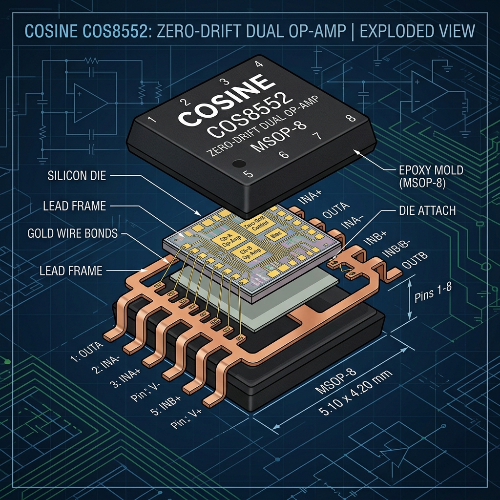
Figure 1: Exploded View of the COS8552 Silicon Die Showing Auto-Zero Chopping Circuitry and Output Stage
This article provides a comprehensive deep-dive into the COS8552's internal architecture, its parametric advantages in the competitive landscape, and critical application design guidelines for maximizing performance in industrial environments.
Zero-drift amplifiers like the COS8552 represent a paradigm shift in analog design. In legacy systems, engineers often had to choose between high bandwidth, low offset, or low noise. The chopper-stabilized architecture breaks these trade-offs by continuously nulling the offset at high frequencies. This active correction mechanism operates entirely transparently to the user, presenting the amplifier simply as an exceptionally perfect analog building block. The implications for system design are profound: sensor nodes can now operate for years in extreme environments without requiring periodic recalibration to compensate for aging or thermal drift. The COS8552's ability to maintain its specifications across the full automotive and industrial temperature range ($-40^\circ\text{C}$ to $+125^\circ\text{C}$) ensures that an analog front-end designed in the lab performs exactly the same in a freezing remote pipeline monitoring station or a sweltering factory floor. This uncompromising consistency is the hallmark of Cosine Nanoelectronics' commitment to high-performance precision silicon.
2. Parametric Benchmark: Setting the Standard
The selection of a precision operational amplifier is governed by a strict matrix of error budgets. Engineers must account for initial offset, temperature drift, common-mode rejection, and power supply rejection to determine the total unadjusted error (TUE) of the system. Table 1 presents a detailed parametric benchmark of the COS8552 against its primary competitors in the zero-drift category.
| Parameter | COS8552 (Cosine) | OPA2188 (TI) | ADA4522-2 (ADI) | LTC2052 (Linear) | Max44251 (Maxim) |
|---|---|---|---|---|---|
| Input Offset Voltage (Vos max) | 5 uV | 25 uV | 5 uV | 3 uV | 6 uV |
| Offset Voltage Drift (max) | 0.05 uV/C | 0.03 uV/C | 0.015 uV/C | 0.03 uV/C | 0.05 uV/C |
| Supply Voltage Range | 2.2V to 5.5V | 4V to 36V | 4.5V to 55V | 2.7V to 7V | 2.7V to 20V |
| CMRR (min) | 120 dB | 120 dB | 145 dB | 115 dB | 135 dB |
| PSRR (min) | 130 dB | 120 dB | 140 dB | 115 dB | 130 dB |
| Gain Bandwidth (GBW) | 2.5 MHz | 2 MHz | 2.7 MHz | 3 MHz | 10 MHz |
| Input Bias Current (max) | 150 pA | 600 pA | 150 pA | 150 pA | 300 pA |
| Slew Rate | 1.2 V/us | 0.8 V/us | 1.3 V/us | 2 V/us | 8 V/us |
The data reveals that the COS8552 holds its ground firmly among the industry's elite precision amplifiers. Its $5\,\mu\text{V}$ maximum offset voltage and $0.05\,\mu\text{V}/^\circ\text{C}$ drift rival or exceed the specifications of parts costing significantly more. The device truly shines in its dynamic error rejection capabilities, boasting a Common-Mode Rejection Ratio (CMRR) of $120\,\text{dB}$ and a Power Supply Rejection Ratio (PSRR) of $130\,\text{dB}$. These figures are not mere datasheet novelties; they are absolute necessities when amplifying millivolt-level sensor signals in electrically hostile environments fraught with ground loops and switching power supply noise.
Furthermore, the COS8552 achieves a Gain-Bandwidth Product (GBW) of $2.5\,\text{MHz}$ while consuming only a fraction of the quiescent current associated with wideband precision amplifiers. This excellent speed-to-power ratio makes it highly suitable for portable, battery-operated instrumentation where every microampere is scrutinized. When compared to the OPA2188, the COS8552 provides equivalent precision but with the distinct advantage of a lower operating supply voltage range down to $2.2\,\text{V}$, seamlessly interfacing with modern $3.3\,\text{V}$ and $2.5\,\text{V}$ mixed-signal microcontrollers without requiring level shifting.
The $1.2\,\text{V}/\mu\text{s}$ slew rate ensures that multiplexed data acquisition systems can rapidly settle to 16-bit or 24-bit accuracy following channel switching, preventing inter-channel crosstalk and maintaining high sample throughput in multi-sensor industrial programmable logic controllers (PLCs).
3. Internal Architecture: The Magic of Chopping
To fully appreciate the performance of the COS8552, one must delve into the mechanics of its auto-zero, chopper-stabilized architecture. Unlike a standard linear amplifier, which relies on large input transistor geometries and laser trimming to minimize mismatch (offset), the COS8552 utilizes a continuous time-domain sampling technique to actively cancel both initial offset and its subsequent temperature drift.
The core topology consists of a main amplifier and a secondary "nulling" amplifier. An internal high-frequency oscillator drives a set of precision CMOS switches. During the first phase of the clock cycle, the nulling amplifier measures the inherent input offset voltage of the main amplifier and stores the required correction voltage on an internal holding capacitor. In the second phase, this correction voltage is applied to an auxiliary input of the main amplifier, effectively subtracting the offset to exactly zero. This process repeats hundreds of thousands of times per second.
The profound secondary benefit of this chopping action is the elimination of 1/f (flicker) noise. In the frequency domain, 1/f noise dominates the low-frequency spectrum below a certain "corner frequency." The chopping mechanism effectively modulates this low-frequency noise (and the DC offset) up to the high chopping frequency. Once shifted to the high-frequency domain, this noise is easily filtered out by the amplifier's own internal frequency compensation and subsequent low-pass filtering stages. The result is a noise spectral density that remains flat (white noise) all the way down to DC.
Figure 2: Micro-miniature MSOP-8 Package Ideal for Space-Constrained 4-20mA Sensor Transmitters
Engineers must be mindful, however, of "chopper artifacts"—tiny voltage spikes at the input terminals synchronous with the internal clock. While the COS8552 employs advanced charge-injection cancellation techniques to minimize these artifacts, highly sensitive designs may benefit from a simple external RC low-pass filter placed just ahead of the inputs to prevent these high-frequency components from interacting with high-impedance sensors or aliasing into analog-to-digital converters (ADCs).
4. Comprehensive Noise Analysis and Equations
In high-resolution systems, noise is the ultimate limit on dynamic range. For the COS8552, the noise performance is vastly simplified by the absence of 1/f noise. The total RMS voltage noise ($V_{rms}$) integrated over a specific bandwidth can be calculated precisely.
The general equation for broadband noise voltage is:
$$V_{rms} = E_n \cdot \sqrt{BW_n}$$
Where $E_n$ is the amplifier's broadband voltage noise spectral density (typically expressed in $\text{nV}/\sqrt{\text{Hz}}$), and $BW_n$ is the equivalent noise bandwidth of the circuit. For a simple first-order low-pass filter, the noise bandwidth is related to the $-3\,\text{dB}$ signal bandwidth ($f_c$) by a factor of $\pi/2$ or approximately $1.57$:
$$BW_n = 1.57 \cdot f_c$$
For example, if the COS8552 (with an assumed $E_n = 22\,\text{nV}/\sqrt{\text{Hz}}$) is used in a circuit with a $10\,\text{kHz}$ low-pass filter, the noise bandwidth is $15.7\,\text{kHz}$. The total integrated RMS noise contributed by the amplifier would be:
$$V_{rms} = 22\,\text{nV}/\sqrt{\text{Hz}} \cdot \sqrt{15,700\,\text{Hz}} \approx 2.75\,\mu\text{V}_{rms}$$
This exceedingly low noise floor allows for the direct amplification of minute signals without burying them in amplifier-generated hiss. It is crucial to remember that in high-precision circuits, the thermal noise (Johnson-Nyquist noise) of the external feedback and source resistors can easily dominate the amplifier's intrinsic noise. The thermal noise of a resistor is given by:
$$V_R = \sqrt{4 \cdot k \cdot T \cdot R \cdot BW_n}$$
To fully leverage the ultra-low noise performance of the COS8552, engineers must carefully optimize the surrounding passive network, selecting resistor values that are low enough to minimize thermal noise, yet high enough to prevent excessive power dissipation and loading of the amplifier output.
5. Pinout Configuration and PCB Layout Rules
The COS8552 adheres strictly to the industry-standard dual operational amplifier pinout, enabling frictionless migration for existing designs. Table 2 details the pin configuration alongside critical layout considerations.
| Pin Number | Pin Name | Type | Function | PCB Design Consideration |
|---|---|---|---|---|
| 1 | OUT A | Output | Amplifier A Output | Keep trace capacitance low (< 50pF) to maintain phase margin |
| 2 | -IN A | Input | Inverting Input A | Guard ring recommended for high-impedance sensor inputs |
| 3 | +IN A | Input | Non-Inverting Input A | Match input impedances to minimize bias current errors |
| 4 | V- | Power | Negative Supply / GND | Solid ground plane connection required for single-supply |
| 5 | +IN B | Input | Non-Inverting Input B | Match input impedances to minimize bias current errors |
| 6 | -IN B | Input | Inverting Input B | Guard ring recommended for high-impedance sensor inputs |
| 7 | OUT B | Output | Amplifier B Output | Keep trace capacitance low (< 50pF) to maintain phase margin |
| 8 | V+ | Power | Positive Supply | Bypass with 0.1uF and 10uF ceramic capacitors directly at pin |
However, achieving sub-microvolt precision requires far more than just connecting the pins. PCB layout for zero-drift amplifiers must be treated with the same rigor as high-frequency RF design, focusing predominantly on minimizing parasitic thermocouples and leakage currents.
A parasitic thermocouple is formed wherever two dissimilar metals join (e.g., copper trace to solder, solder to component lead). A temperature gradient across these junctions generates a Seebeck voltage that can easily exceed the amplifier's intrinsic offset voltage. To mitigate this, the layout must be thermally symmetric. Keep heat-generating components (like power regulators) far away from the COS8552. Ensure that both input traces (+IN and -IN) are routed parallel to each other, using identical lengths, identical trace widths, and crossing the same thermal gradients, so any induced thermocouple voltages appear as a common-mode signal which the amplifier can reject.
Furthermore, leakage currents across the FR-4 PCB substrate can introduce significant errors when interfacing with high-impedance sensors (like pH probes). Surface contamination from flux residue or humidity can create parasitic resistance paths between the input pins and adjacent high-voltage nodes. Implementing a "guard ring"—a copper trace completely encircling the sensitive input pins and driven to the same potential as those pins—intercepts these leakage currents, preserving the amplifier's ultra-low $150\,\text{pA}$ input bias current specification.
6. Application: RTD Bridge Amplifiers
Resistance Temperature Detectors (RTDs), such as the PT100, provide highly linear and stable temperature measurements by changing their resistance relative to temperature. A PT100 has a resistance of $100\,\Omega$ at $0^\circ\text{C}$ and changes by approximately $0.385\,\Omega/^\circ\text{C}$. This minute variation demands exceptionally precise signal conditioning.
The COS8552 is perfectly suited for amplifying the microvolt-level differential output of a Wheatstone bridge containing an RTD. In a typical instrumentation amplifier configuration built with two or three COS8552 amplifiers, the ultra-low offset voltage ensures that the zero-degree calibration point is exact without requiring a manual trimming potentiometer. More importantly, the $0.05\,\mu\text{V}/^\circ\text{C}$ maximum drift guarantees that as the electronics enclosure heats up, the amplifier does not introduce a false temperature reading into the measurement.
When designing the RTD bridge, the excitation current must be kept low (typically $< 1\,\text{mA}$) to prevent self-heating of the RTD element, which would skew the measurement. This low excitation current results in a very small differential voltage swing, maximizing the need for the COS8552's $120\,\text{dB}$ CMRR to reject common-mode noise coupled onto the sensor cables in electrically noisy factory environments.
Figure 3: COS8552 Deployed in a Multi-Channel PLC Analog Input Module Architecture
By pairing the COS8552 with highly stable $0.1\%$ thin-film resistors for the bridge completion and gain-setting networks, engineers can achieve instrumentation-grade temperature measurement systems capable of resolving fractions of a degree over a massive operational temperature spectrum.
7. Application: Thermocouple Signal Conditioning
Thermocouples generate a voltage proportional to the temperature difference between the hot junction (measurement point) and the cold junction (connection point). For a Type-K thermocouple, the Seebeck coefficient is roughly $41\,\mu\text{V}/^\circ\text{C}$. Resolving a $0.1^\circ\text{C}$ temperature change therefore requires amplifying a signal of just $4.1\,\mu\text{V}$.
Legacy linear amplifiers with offsets in the hundreds of microvolts would completely bury this signal, requiring continuous software-based auto-zeroing loops that consume valuable MCU cycles and delay measurement updates. The COS8552's native $5\,\mu\text{V}$ offset represents less than $0.15^\circ\text{C}$ of absolute uncalibrated error, providing unprecedented out-of-the-box accuracy for thermal monitoring systems.
In thermocouple applications, the COS8552 is typically configured as a high-gain non-inverting amplifier. The differential cold-junction compensation (CJC) signal, usually derived from an adjacent precision temperature sensor like an RTD or silicon bandgap sensor, can be summed directly into the amplifier's feedback node or handled digitally by the MCU. The COS8552's high PSRR ($130\,\text{dB}$) ensures that ripple from the system's power supply does not translate into phantom temperature fluctuations, a critical factor when the sensor data is fed into a PID loop controlling high-power heating elements.
Because thermocouple cables can act as long antennas, picking up RFI and EMI from motor drives and contactors, adding a passive RC low-pass filter immediately prior to the COS8552's input pins is highly recommended to suppress out-of-band high-frequency noise before it can be rectified by the amplifier's input stage.
8. Application: 4-20mA Current Loop Transmitters
The 4-20mA current loop remains the undisputed king of analog industrial communication, offering robust, noise-immune signal transmission over miles of twisted-pair wire. In a 2-wire transmitter design, the entire sensor circuit (including the microcontroller, sensor excitation, and the amplifier) must operate entirely from the power drawn directly from the loop, limiting the total allowable quiescent budget to less than $4\,\text{mA}$.
The COS8552's wide operating voltage range ($2.2\,\text{V}$ to $5.5\,\text{V}$) and highly efficient current consumption profile make it an ideal choice for the analog front-end of these power-starved smart transmitters. It is frequently employed as the precision error amplifier within the voltage-to-current (V/I) conversion stage.
In this architecture, a precision digital-to-analog converter (DAC) provides the target voltage to the COS8552, which drives an external high-voltage bipolar transistor or MOSFET to regulate the exact loop current flowing through a precision sense resistor. The COS8552's zero-drift topology ensures that the V/I conversion remains absolutely stable across the extreme temperature variations experienced by field-mounted transmitters, guaranteeing that $4.000\,\text{mA}$ always represents exactly zero scale, and $20.000\,\text{mA}$ always represents full scale, year after year.
Furthermore, the COS8552 is available in an ultra-compact MSOP-8 package, saving critical board space in the heavily space-constrained cylindrical enclosures typical of process control transmitters.
9. Application: Precision Low-Side Current Shunt Sensing
Accurate current measurement is critical for battery management systems (BMS), motor torque control, and power supply diagnostics. A common technique involves placing a very small, low-inductance shunt resistor (e.g., $1\,\text{m}\Omega$) in series with the load path and amplifying the resultant voltage drop.
To minimize $I^2R$ power dissipation and thermal management issues, the shunt resistor value must be kept as low as possible. Consequently, a $10\,\text{A}$ load current passing through a $1\,\text{m}\Omega$ shunt generates a mere $10\,\text{mV}$ differential signal. The COS8552's $5\,\mu\text{V}$ maximum offset voltage equates to a negligible $5\,\text{mA}$ error offset in this $10\,\text{A}$ system (a $0.05\%$ absolute error), making it vastly superior to standard amplifiers that would require complex calibration routines.
When implementing the COS8552 for low-side current sensing, it is often configured as a differential amplifier to reject ground bounce and trace resistance errors. The high CMRR of the COS8552 effectively ignores the common-mode voltage fluctuations caused by high-current switching transients in the ground return path. It is imperative to use strict Kelvin (4-wire) connections directly to the physical pads of the shunt resistor. Any copper trace resistance included in the measurement path will introduce massive temperature-dependent errors due to the high temperature coefficient of copper (approx $3,900\,\text{ppm}/^\circ\text{C}$). By combining Kelvin connections, stable thin-film feedback resistors, and the zero-drift COS8552, engineers can forge highly accurate current monitoring systems capable of operating reliably in harsh automotive and industrial power applications.
10. FAE Troubleshooting and Support
Even with the most precise silicon, achieving sub-microvolt accuracy in the field requires meticulous system design. Table 4 summarizes common failure modes observed by Cosine Nanoelectronics' Field Application Engineering (FAE) team when supporting high-precision designs, along with proven diagnostic and corrective actions.
| Observed Symptom | Potential Root Cause | Diagnostic Step | Corrective Action |
|---|---|---|---|
| Output ringing or oscillation | Excessive capacitive load | Check output node capacitance on scope | Add isolation resistor (e.g., 50 ohm) in series with output |
| Unexplained DC offset shift | Thermocouple effects on PCB | Cool PCB with spray; observe offset | Symmetrize layout, use identical metals for input traces |
| Excessive 1/f noise | Chopping frequency interference | Perform FFT on output signal | Add active low-pass filter to attenuate chopping artifacts |
| Output saturated near rail | Input common-mode violation | Measure V+ and V- inputs relative to supply | Ensure inputs remain strictly within specified CMVR limits |
Figure 4: The Standard SOP-8 Package Enabling Direct PCB Migration from TI OPA2188 and ADI ADA4522-2
A frequent challenge involves output ringing when driving capacitive loads, such as the input capacitance of an unbuffered analog-to-digital converter (ADC) or long coaxial cables. While the COS8552 is stable for moderate capacitive loads, excessive capacitance can erode the phase margin, leading to oscillation. Inserting a small isolation resistor (e.g., $20\,\Omega$ to $100\,\Omega$) closely adjacent to the amplifier's output pin effectively decouples the load capacitance, restoring stability.
Another subtle issue is the appearance of unexplained DC offset shifts that correlate with ambient airflow or enclosure heating. This is almost universally traced back to parasitic thermocouples on the PCB. Diagnosing this requires isolating the PCB from air currents (e.g., covering it with a box) and observing if the offset stabilizes. Redesigning the layout to ensure absolute thermal symmetry around the input pins is the definitive solution.
11. Ordering Options and Package Portfolio
To accommodate a wide array of manufacturing requirements and physical constraints, the COS8552 is available in several industry-standard packaging options:
- COS8552S: The standard 8-pin SOP-8 (Small Outline Package) format. This package is the universal standard for precision amplifiers, providing a direct pin-for-pin footprint match for upgrading legacy designs currently utilizing the OPA2188 or ADA4522-2 without any PCB modifications.
- COS8552MS: The miniature 8-pin MSOP-8 (Mini Small Outline Package). Taking up only half the board space of the SOP-8, this package is the preferred choice for densely populated sensor transmitters, portable medical instrumentation, and compact multi-channel PLC I/O modules.
Both package variants are manufactured using RoHS-compliant materials and feature pure matte-tin plating for excellent solder joint reliability. They are fully qualified over the extended industrial temperature range of $-40^\circ\text{C}$ to $+125^\circ\text{C}$ and undergo rigorous MSL (Moisture Sensitivity Level) testing to ensure they withstand the rigors of modern high-temperature lead-free reflow profiles.
12. Conclusion
The COS8552 dual precision zero-drift chopper op-amp redefines the boundaries of industrial signal conditioning. By offering sub-$5\,\mu\text{V}$ offset, virtually unmeasurable temperature drift, and massive $130\,\text{dB}$ power supply rejection, it empowers design engineers to capture the most elusive microvolt-level signals in the harshest environments on earth.
Whether you are designing a high-resolution 4-20mA RTD transmitter for a chemical refinery, a precision low-side current shunt monitor for an electric vehicle battery management system, or a multi-channel thermocouple interface for factory automation, the COS8552 delivers the uncompromising metrological accuracy required for mission-critical measurements.
Its flawless drop-in compatibility with the TI OPA2188 and ADI ADA4522-2 means that upgrading your system's performance and solidifying your supply chain has never been easier. As the world pushes for ever-tighter control loops and higher resolution data acquisition, the fundamental requirement for a pristine analog front-end is paramount. The COS8552 guarantees that your signal integrity remains perfect from the sensor to the ADC, regardless of thermal stress or electrical interference.
Experience the zero-drift advantage today. Request comprehensive datasheets, download our highly accurate SPICE simulation models, or order engineering evaluation samples. For direct technical consultation and layout review, contact the Cosine Nanoelectronics application engineering team at sales@cosinechips.com or reach out immediately at +86 159 5954 3210.
Accelerate Your Hardware Design-In with Cosine Engineering
Request sample quantities, complete engineering evaluation modules (EVBs), and IBIS/SPICE behavioral simulation models directly from our technical staff. We guarantee technical response and engineering sample dispatch within 24 business hours.