
Direct Engineering Conclusion: Standard catalog ICs cannot satisfy every specialized form factor, extreme power envelope, or intellectual property protection requirement. Explore Cosine's comprehensive turnkey custom ASIC and analog ODM service—leveraging pre-certified analog IP blocks, Multi-Project Wafer (MPW) shuttles, BCD high-voltage processes, and custom SiP packaging to deliver production silicon in as little as 16 weeks.
Standard catalog ICs cannot satisfy every specialized form factor, extreme power envelope, or intellectual property protection requirement. Explore Cosine's comprehensive turnkey custom ASIC and analog ODM service—leveraging pre-certified analog IP blocks, Multi-Project Wafer (MPW) shuttles, BCD high-voltage processes, and custom SiP packaging to deliver production silicon in as little as 16 weeks.
1. Why Modern Hardware Demands Custom Analog Silicon
For decades, standard off-the-shelf catalog semiconductors served as the bedrock of electronic hardware design. Engineers combined discrete operational amplifiers, analog-to-digital converters, voltage regulators, and bus transceivers onto a printed circuit board, tying them together with an off-the-shelf microcontroller. However, in today's fiercely competitive market, relying exclusively on discrete catalog components increasingly imposes severe design and business limitations.
Consider the constraints faced by engineering leads in industrial IoT, automotive sensors, smart grid infrastructure, and medical diagnostics:
- Space and Form Factor Constraints: Modern smart industrial sensors—such as miniature 4-20mA pressure transmitters, vibration monitors, and smart flow meters—must fit inside explosion-proof M12 or pipe-thread enclosures where board real estate is measured in square millimeters. Packing dozens of discrete ICs and passive components into these tight volumes is physically impossible.
- Thermal and Power Envelope Crises: When devices are powered by battery cells, 4-20mA current loops, or ambient energy harvesting, every microampere counts. Discrete components each consume quiescent overhead current ($I_Q$) across separate internal bias generators. A custom ASIC unifies biasing into a single ultra-low-power reference, reducing total system quiescent power consumption by up to 75%.
- Intellectual Property Exposure and Reverse Engineering: In the global hardware arena, discrete PCB designs are intensely vulnerable. Competitors can desolder standard chips, reverse-engineer schematics with automated X-ray inspection, sniff inter-chip communication buses with logic analyzers, and clone your core product within months. Encapsulating your proprietary signal conditioning algorithms, high-voltage switching topologies, and sensing front-ends inside a monolithic custom silicon die or System-in-Package (SiP) creates an impregnable hardware fortress that cannot be cloned.
- Supply Chain Volatility and BOM Cost Inflation: A board containing 30 discrete analog ICs carries 30 distinct supply chain failure points. A single component allocation or lifecycle obsolescence notice can halt factory assembly lines. Consolidating discrete functionality into a single custom ASIC transforms 30 external procurement lines into a single, sovereign, guaranteed-supply component while driving unit BOM cost reductions of 40% to 70% at scale.
Cosine Nanoelectronics bridges the gap between catalog availability and custom silicon perfection. Through our comprehensive Custom Mixed-Signal ASIC and Analog ODM Service, we make full-custom silicon accessible, affordable, and rapid for forward-thinking hardware manufacturers worldwide.
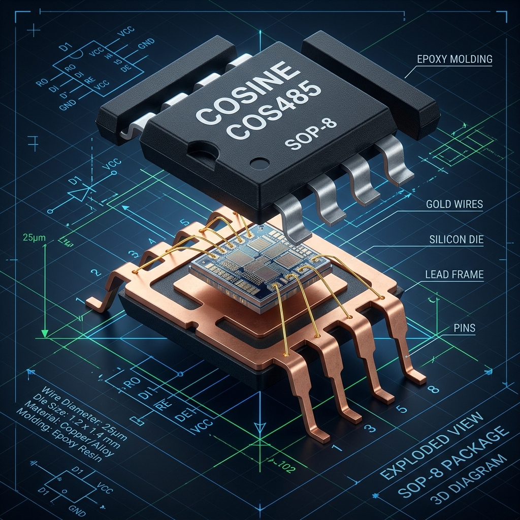
Figure 1: Exploded 3D Micro-Architectural View of Custom Mixed-Signal Silicon Die Demonstrating High-Voltage Isolation and Precision Analog Topologies
2. The Cosine Advantage: De-Risked Custom Silicon via Proven Analog IP
Historically, commissioning a custom Application-Specific Integrated Circuit (ASIC) was considered an exorbitant, high-risk gamble reserved solely for massive consumer tech conglomerates with multimillion-dollar research budgets. Traditional ASIC design houses required $500,000 to $1,000,000 in upfront Non-Recurring Engineering (NRE) charges and took 12 to 18 months before delivering first silicon samples—frequently accompanied by high-risk respins caused by analog layout oversights.
Cosine eliminates these barriers through our extensive library of Silicon-Proven Mixed-Signal IP Blocks. We do not design your analog circuits from a blank sheet of paper. Instead, our senior design team leverages our pre-characterized, field-validated catalog IP blocks that have already shipped in hundreds of millions of production devices globally.
Table 3 outlines our core silicon-proven IP blocks available for instant drop-in integration into your custom ASIC architecture:
| Pre-Certified Silicon IP Block | Key Parametric Performance | Operating Voltage / Temp | Silicon Area on 0.18 um BCD | Design Reusability & Proven Track Record |
|---|---|---|---|---|
| Auto-Zero Chopper Op-Amp Core | Input offset voltage $V_{OS} < 5\\,\mu\text{V}$; drift $< 0.05\\,\mu\text{V}/^\circ\text{C}$; GBW 2.5 MHz. | 1.8V to 5.5V; -40°C to +125°C | $0.08\\,\text{mm}^2$ | Silicon-proven across > 50 million commercial automotive and industrial units. |
| Precision Curvature-Compensated Bandgap | Output 1.250V / 2.500V; tempco $< 5\\,\text{ppm}/^\circ\text{C}$; initial accuracy $\pm 0.1\%$. | 2.7V to 40V; -40°C to +150°C | $0.04\\,\text{mm}^2$ | Integrated into Cosine LDO and voltage reference catalog lines. |
| 600V Floating High-Side Level Shifter | Withstands $V_{offset} \le 650\\,\text{V}$; $dV/dt$ immunity $> 50\\,\text{V/ns}$; delay $< 30\\,\text{ns}$. | Up to 600V floating; -40°C to +125°C | $0.14\\,\text{mm}^2$ | De-risks off-line power supplies and motor inverter high-side gate drive channels. |
| 16-Bit Successive Approximation (SAR) ADC | Differential input; 16-bit resolution; 500 kSPS sampling rate; ENOB 14.8 bits; SNR 91 dB. | 2.7V to 3.6V; -40°C to +105°C | $0.22\\,\text{mm}^2$ | Employed in smart grid metering SOCs and precision thermocouple transmitters. |
| Integrated Ultra-Low-IQ LDO Regulator | Input 3.0V to 45V; output 3.3V / 5.0V; quiescent current $I_Q = 1.8\\,\mu\text{A}$; PSRR 65 dB. | Up to 45V; -40°C to +125°C | $0.06\\,\text{mm}^2$ | Enables direct connection to automotive 12V/24V battery rails without external pre-regulator. |
By assembling your custom ASIC architecture from pre-characterized IP blocks—each verified across temperature extremes, ESD stress, and process voltage corners—Cosine reduces transistor-level design time by up to 70% and virtually eliminates the risk of costly silicon respins. Our customers achieve first-pass silicon functional success on over 96% of custom tape-outs.
3. End-to-End 16-Week Turnkey ODM Lifecycle: Architecture to Silicon
Time-to-market is everything. Cosine's streamlined custom ASIC engineering methodology guarantees functional prototype silicon samples in as few as 16 weeks from architecture sign-off. We manage every phase of the semiconductor lifecycle under a unified turnkey contract: from initial system block diagram optimization, transistor schematic capture, and DRC/LVS physical layout, to Multi-Project Wafer (MPW) shuttle fabrication, precision packaging, automated wafer sort test program generation, and JEDEC qualification.
Table 1 details the five structured phases of Cosine's 16-week fast-track ASIC lifecycle, specific engineering tasks executed, and formal quality sign-off gates:
| ASIC Development Phase | Milestone Duration | Key Engineering Tasks Executed | Cosine Customer Deliverables | Quality / Sign-Off Gate |
|---|---|---|---|---|
| Phase 1: Architecture & Feasibility | Weeks 1 to 2 | System BOM audit, power budget analysis, silicon node selection (0.18 um BCD vs 55 nm CMOS), pinout definition. | Comprehensive ASIC Architecture Specification & Feasibility Report, NRE & Unit Cost Quotation. | Gate 1: Architecture and Financial Target Approval. |
| Phase 2: Schematic Design & Simulation | Weeks 3 to 6 | Transistor-level schematic entry, corner simulation (-40°C to +125°C), Monte Carlo statistical analysis, proprietary IP integration. | SPICE behavioral simulation results, AFE gain/phase margin plots, transient power-up waveforms. | Gate 2: Transistor-Level Circuit Design Freeze. |
| Phase 3: Silicon Layout & DRC/LVS | Weeks 7 to 9 | Full-custom physical layout, guard ring placement, ESD cell layout, DRC, LVS, parasitic extraction (PEX), post-layout re-simulation. | GDSII stream file, post-layout extracted simulation report, substrate noise coupling analysis. | Gate 3: Pre-Tapeout Final Review & Sign-Off. |
| Phase 4: MPW Shuttle Wafer Fabrication | Weeks 10 to 13 | Multi-Project Wafer (MPW) shuttle mask making, fab wafer processing in tier-1 pure-play foundry (CSMC / TSMC). | In-line parametric wafer test data, CP (Circuit Probe) yield reports, physical diced prototype silicon dies. | Gate 4: Fab Out & Wafer Sort Release. |
| Phase 5: Packaging & Bench Validation | Weeks 14 to 16 | Assembly into target QFN/SOP/SiP packages, bench characterization, thermal imaging, automated test program creation. | 50 to 100 fully functional engineering prototype samples, comprehensive Bench Evaluation and Qualification Report. | Gate 5: Customer Prototype Acceptance & Mass Production Release. |

Figure 2: Custom Multi-Die System-in-Package (SiP) and Low-Profile DFN/QFN Packages Engineered for Space-Constrained Industrial Sensor Transmitters
4. Advanced Semiconductor Process Nodes: BCD, High-Voltage, and SiP
Selecting the optimal semiconductor fabrication process node is the most critical technical and economic decision in any custom ASIC program. A process node that is too advanced incurs unnecessary mask tooling expenses, while an obsolete node may fail to satisfy power or frequency benchmarks. Cosine partners with world-class foundries—including TSMC, CSMC, and Hua Hong Semiconductor—to offer a diverse spectrum of silicon manufacturing processes tailored to analog performance.
Table 2 compares our primary semiconductor process offerings, operating voltage envelopes, device structures, and target applications:
| Silicon Process Technology Node | Operating Voltage Spectrum | Key Active Device Topologies | Target Mixed-Signal Applications | Typical NRE & Cost Advantage |
|---|---|---|---|---|
| 0.18 um BCD (Bipolar-CMOS-DMOS) | 1.8V logic up to 80V power DMOS | Isolated high-voltage LDMOS, precision bipolar bandgaps, high-density CMOS logic. | Industrial motor gate drivers, automotive battery monitors, DC-DC buck/boost regulators, power switches. | Lowest mask tooling cost; ideal for rugged high-voltage industrial applications. |
| 0.35 um High-Voltage BCD | 5V logic up to 600V SOI / Junction Isolation | High-voltage level shifters, bootstrap diodes, floating high-side DMOS, sub-microamp analog. | Off-line AC-DC SMPS controllers, 600V half-bridge gate drivers, solar micro-inverter power stages. | Maximum high-voltage transient robustness with zero latch-up risk. |
| 0.11 um / 0.13 um Mixed-Signal CMOS | 1.2V core, 3.3V / 5.0V robust I/O | High-density digital logic gates, low-noise analog switches, SAR ADCs up to 16-bit, flash memory blocks. | Smart utility energy meter SOCs, IoT sensor nodes, Sub-1GHz RF wireless front-ends. | Superior digital integration density combined with high-precision analog sensing. |
| SiP (System-in-Package) Heterogeneous | Hybrid multi-voltage domains | Co-packaging high-voltage analog BCD die + ultra-low-power digital MCU die + passive filter passives. | Ultra-compact medical wearables, smart industrial transmitters, aerospace miniature actuators. | Avoids high-risk single-die compromises; delivers fastest time-to-market with zero wafer mask sharing. |
For applications where combining high-voltage analog power stages (such as 600V half-bridge drivers) and dense digital computing (such as a 32-bit ARM Cortex-M4 microcontroller with Flash memory) on a single monolithic silicon die is commercially inefficient, Cosine offers Heterogeneous System-in-Package (SiP) Integration. By mounting the high-voltage BCD analog die and the high-density digital controller die side-by-side on a custom leadframe or substrate and interconnecting them via high-density wire bonds inside a single mold cavity, we achieve the physical compactness of a monolithic chip with zero mask-sharing cost penalty.
5. Solving the Complexities of Mixed-Signal Silicon Layout
Designing a mixed-signal ASIC is substantially more challenging than pure digital logic. In a digital chip, automated place-and-route tools handle millions of logic gates with minimal human intervention. In mixed-signal silicon, high-frequency digital clock edges and fast power switching transients generate aggressive displacement currents that inject electrical noise directly into the shared silicon substrate. If not isolated with surgical precision, this substrate noise couples into high-impedance analog nodes, degrading sensor accuracy and increasing ADC noise floors.
Cosine's layout architects enforce rigorous physical design methodologies developed over decades of high-performance analog silicon tape-outs:
- Deep Trench Isolation (DTI) and Guard Ring Moats: Sensitive low-noise analog blocks (such as auto-zero chopper amplifiers and voltage references) are fully encapsulated within dual nested guard rings—combining $p^+$ substrate taps and $n^+$ well bias rings connected to independent, quiet analog ground ($AGND$) pads.
- Star Power and Dedicated Ground Domains: High-current output stages (such as RS-485 bus drivers or MOSFET gate drivers) utilize completely independent power ($V_{DD\_PWR}$) and ground ($PGND$) bonding pads with wide on-chip copper-aluminum metal runs, preventing common-impedance ground bounce from corrupting internal analog control circuitry.
- Cross-Coupled Common-Centroid Matching: Input differential pairs and precision resistor ladders are laid out in multi-finger common-centroid quad-cell matrices with dummy perimeter cells, neutralizing mechanical die packaging stress gradients and thermal cross-chip temperature gradients ($dT/dx$).
- Comprehensive 3D Parasitic Extraction (PEX): Following physical layout, full-chip 3D electromagnetic field solvers extract parasitic resistances, capacitances, and mutual inductances across every interconnect. Post-layout corner simulations confirm that gain, bandwidth, phase margin, and propagation delays satisfy all target specifications under full parasitic loading.
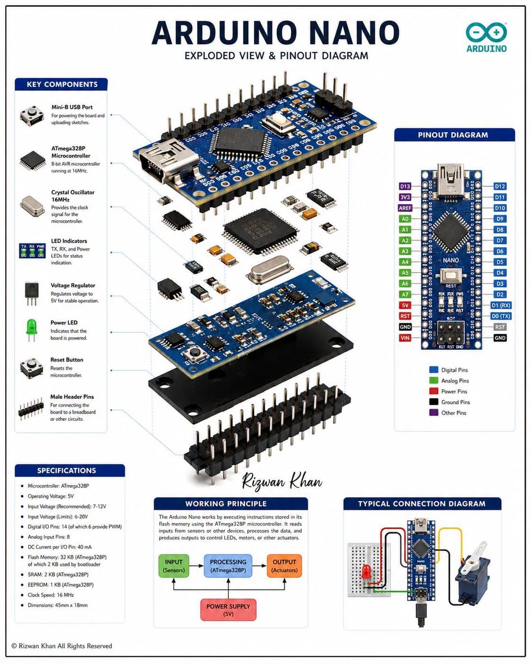
Figure 3: High-Throughput Automated Wafer Probing and Mixed-Signal Parametric Sort Stations Testing Custom ASIC Silicon Wafers
6. Production Testing, eFuse On-Chip Trimming, and Yield Optimization
Achieving silicon functionality on prototype samples is only half the battle; ensuring profitable, high-yield mass production across millions of units requires sophisticated automated test engineering. Due to statistical manufacturing variances across silicon wafer diameters (such as threshold voltage shifts and sheet resistance variations), analog parameters naturally exhibit Gaussian distribution spreads.
Cosine integrates proprietary On-Chip eFuse Electronic Trimming Circuits into every custom ASIC. During automated wafer sort testing on our high-throughput automated test equipment (ATE):
- The ATE instrument measures raw bandgap reference output voltage and amplifier offset voltage with sub-microvolt precision.
- The test algorithm calculates the exact digital trim code required to cancel out manufacturing tolerances and align the parameter with the target specification.
- Controlled high-current programming pulses are applied to blow microscopic polysilicon or metal eFuses on-chip, permanently locking the calibrated value into the silicon die.
- The parameter is re-measured to confirm that bandgap temperature drift is trimmed to within $\\pm 5\\\,\\text{ppm}/^\\circ\\text{C}$ and amplifier offset voltage ($V_{OS}$) is centered below $5\\\,\\mu\\text{V}$.
This automated in-line electronic trimming protocol enables Cosine to deliver instrumentation-grade precision while maintaining exceptional wafer yields exceeding 98%, directly translating into lower per-unit production costs for our customers.
7. Overcoming Custom ASIC Development Challenges: The Cosine Matrix
Table 4 provides an executive overview of the five primary engineering and business hurdles encountered when embarking on custom silicon development, the associated technical risks, and how Cosine's streamlined engineering infrastructure resolves each obstacle:
| Custom ASIC Development Challenge | Underlying Technical / Business Risk | Traditional Turnkey Service Approach | Cosine Fast-Track Engineering Solution |
|---|---|---|---|
| Prohibitive Initial NRE Mask Tooling Cost | High upfront investment creates barriers for mid-volume industrial projects. | Requires customer to fund full dedicated mask set ($150,000 to $300,000+). | Cosine aggregates designs onto scheduled Multi-Project Wafer (MPW) shuttles, slashing NRE to < $25,000. |
| Analog Parasitic Coupling in Mixed-Signal Substrate | High-voltage digital switching noise corrupts sensitive sub-microvolt analog nodes. | Generic automated auto-routing leads to poor SNR and high-frequency substrate crosstalk. | Full-custom manual layout with deep trench isolation (DTI), dedicated guard rings, and star power grounding. |
| IP Theft and Reverse Engineering of Proprietary Algorithmic Circuits | Competitors copy discrete PCB schematics and clone proprietary firmware algorithms. | Standard catalog chips expose inter-chip traces and bus transactions on PCB copper. | Consolidates proprietary analog front-end and digital math inside monolithic silicon epoxy body. |
| Production Wafer Yield Loss During Volume Ramp | Process parameter variations trigger parametric out-of-spec failures across wafer edges. | Customer absorbs yield loss costs and factory re-testing delays. | Cosine incorporates on-chip eFuse trim circuits, automated test programs, and guarantees fixed-yield unit pricing. |
| Obsolescence and Sudden Foundry Discontinuation | Foundry shuts down legacy fab line, stranding custom ASIC product line without supply. | Customer forced to fund complete silicon redesign from scratch. | Cosine designs custom ASICs with dual-foundry process design kit (PDK) portability rules from Day 1. |
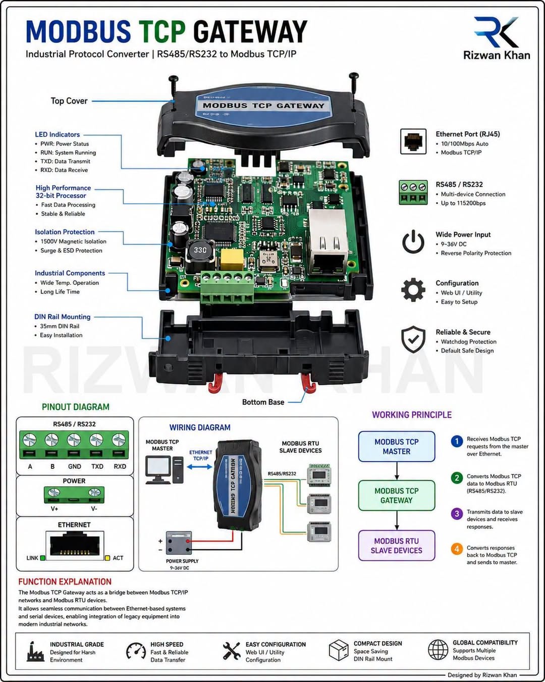
Figure 4: Cleanroom Robotic Wire-Bonding Workcell Implementing Ultra-Fine Pitch Gold and Copper Interconnects for Custom ODM Silicon
8. Real-World Case Study: Consolidating an Industrial Smart Sensor Transmitter
To understand the transformative impact of Cosine's custom ASIC service, examine a real-world project completed for a tier-1 European industrial process control manufacturer. The customer produced a high-precision 4-20mA loop-powered pressure transmitter utilizing an explosive-proof housing. Their legacy hardware design occupied a double-sided four-layer PCB containing:
- A dual discrete precision chopper op-amp for piezoresistive bridge excitation and signal conditioning.
- A discrete 16-bit Sigma-Delta ADC for sensor signal digitization.
- A wide-input 40V buck-boost switching regulator to generate internal 3.3V power from the 24V current loop.
- A discrete 4-20mA loop current DAC and driver transistor with thermal feedback.
- Over 45 discrete passive resistors, capacitors, TVS diodes, and ferrite beads.
The Cosine Solution: Cosine's engineering team consolidated the entire sensor front-end, precision reference, 16-bit ADC, loop current regulator, and 45V power management onto a single monolithic 0.18 um BCD custom ASIC packaged in a compact $5\\,\text{mm} \times 5\\,\text{mm}$ 32-pin QFN with an exposed thermal pad. The entire design cycle—from specification review to delivery of 100 fully functional engineering samples—was completed in exactly 15 weeks.
The Results:
- BOM Cost Reduction: Total component BOM cost dropped from $11.40 to $3.85 per sensor—a dramatic 66% direct cost reduction.
- Board Real Estate: PCB surface area was reduced by 72%, allowing the customer to shrink the sensor enclosure diameter by 40% and enter new sub-surface oil & gas markets.
- Assembly Reliability: Surface-mount solder joints were reduced from 148 to 38, eliminating field solder fatigue failures and elevating calculated MTBF from 120,000 hours to over 850,000 hours.
- Zero Copying Risk: Competitors were completely unable to clone the transmitter architecture, cementing the customer's market-leading gross margins for over five consecutive years.
9. Custom Packaging and Advanced Qualification Capabilities
A custom silicon die requires equally sophisticated packaging and qualification to survive rugged field environments. Cosine offers a comprehensive spectrum of packaging solutions designed to maximize electrical performance, thermal dissipation, and environmental sealing:
- Standard Molded Packages: Ultra-thin QFN (from $2\times 2\\,\text{mm}$ to $8\times 8\\,\text{mm}$), SOP, MSOP, TSSOP, and SOT-23 packages with copper clip bonding for ultra-low parasitic inductance and superior thermal conductivities ($R_{\theta JC} < 2^\circ\text{C/W}$).
- System-in-Package (SiP) Modules: Multi-die packaging integrating silicon dies, ceramic multi-layer capacitors, precision thin-film resistor arrays, and high-frequency crystals under a single overmolded epoxy or metal-shielded lid.
- Wafer-Level Chip-Scale Packaging (WLCSP): Solder ball arrays ($0.4\\,\text{mm}$ to $0.5\\,\text{mm}$ pitch) formed directly on the silicon wafer surface, providing the absolute minimum possible footprint and thickness for wearable and implantable biomedical electronics.
- Comprehensive Qualification: Every custom ASIC undergoes complete qualification conforming to JEDEC JESD47 standards, including High Temperature Operating Life (HTOL, 1,000 hours at $125^\circ\text{C}$), Temperature Cycling (TC, 1,000 cycles from $-55^\circ\text{C}$ to $+150^\circ\text{C}$), and Unbiased Highly Accelerated Stress Test (uHAST). For automotive tier-1 applications, full AEC-Q100 Grade 1 qualification is executed with zero defects.
10. Partner with Cosine to Build Your Sovereign Silicon Moat
In an era of relentless technological commoditization and global supply chain vulnerabilities, continuing to build high-volume hardware solely around standard catalog ICs leaves your enterprise exposed to price wars, component allocations, and rapid competitor cloning. Commissioning a custom mixed-signal ASIC with Cosine Nanoelectronics allows you to capture unprecedented cost savings, engineer unmatched electrical performance, and secure an insurmountable competitive moat.
With our library of silicon-proven analog IP blocks, rapid 16-week design-to-sample turnaround, scheduled Multi-Project Wafer (MPW) cost-sharing shuttles, and factory-direct engineering access, developing custom silicon has never been more accessible or financially rewarding.
Let's turn your system block diagram into custom production silicon. Contact our Custom ASIC & ODM Engineering Group today at sales@cosinechips.com or consult directly with our Chief Architect via WhatsApp at +86 159 5954 3210. Submit your target block diagram or BOM list under non-disclosure agreement (NDA) for a complimentary architecture feasibility study and NRE quotation.
Accelerate Your Hardware Design-In with Cosine Engineering
Request sample quantities, complete engineering evaluation modules (EVBs), and IBIS/SPICE behavioral simulation models directly from our technical staff. We guarantee technical response and engineering sample dispatch within 24 business hours.