
Direct Engineering Conclusion: A strategic and technical deep dive into Cosine's dual-foundry BCD manufacturing architecture. Learn how our dual-source 8-inch and 12-inch wafer allocation, defect density control (D0 < 0.08/cm²), and 8-12 week delivery cycles permanently insulate global OEMs from geopolitical allocations and single-fab shutdowns.
A strategic and technical deep dive into Cosine's dual-foundry BCD manufacturing architecture. Learn how our dual-source 8-inch and 12-inch wafer allocation, defect density control (D0 < 0.08/cm²), and 8-12 week delivery cycles permanently insulate global OEMs from geopolitical allocations and single-fab shutdowns.
1. The Geopolitical and Economic Imperative of Semiconductor Resilience
Over the past decade, the global electronics industry has endured unprecedented disruptions. Semiconductor supply chains, once taken for granted as frictionless and infinitely scalable, revealed systemic vulnerabilities to geopolitical tensions, regional trade tariffs, natural disasters, and unilateral export controls. Hardware manufacturers across industrial automation, automotive electronics, and clean energy infrastructure experienced devastating component shortages, with delivery lead times for basic analog interface ICs, operational amplifiers, and power management devices extending from normal 8-week windows to an astonishing 52 weeks or longer.
In response to these catastrophic vulnerabilities, enterprise procurement executives and chief technology officers have fundamentally re-evaluated their component sourcing criteria. Technical excellence and cost efficiency remain non-negotiable, but they are no longer sufficient on their own. Today, the paramount requirement is Supply Chain Sovereignty and Zero-Disruption Delivery Resilience. Cosine Nanoelectronics was architected from its inception to eliminate single-point supply failures by establishing a robust, dual-foundry Bipolar-CMOS-DMOS (BCD) manufacturing model spanning state-of-the-art 8-inch and 12-inch fabrication lines.
Figure 1: Automated 300mm (12-inch) Wafer Stepper and Photolithography Bay Operating Under ISO Class 3 Cleanroom Environment
2. The Dual-Foundry Architectural Philosophy: Eliminating Single Points of Failure
Most fabless semiconductor companies operate under a perilous operational model: they qualify a single product family at a single commercial foundry partner. While this approach minimizes initial non-recurring engineering (NRE) tooling costs and mask-set investments, it leaves the company and its customers completely hostage to that single facility. A transformer fire, chemical contamination incident, municipal water restriction, or localized power blackout at that one fabrication plant immediately halts wafer starts, triggering a multi-quarter supply freeze that cascades into global customer assembly line shutdowns.
Cosine Nanoelectronics completely rejects this fragile paradigm. Under our Dual-Foundry Resilience Architecture, every core product line in our portfolio—from our RS-485 transceiver family (COS485, COS3485, COS13487) to our precision chopper operational amplifiers (COS8552) and 600V gate drivers (COS2103)—is systematically co-developed and qualified across two independent, tier-one domestic semiconductor foundries:
- Foundry Partner Alpha (High-Yield 8-Inch BCD Line): Specializes in mature, cost-optimized 0.18µm BCD processes. This line features fully amortized tooling, mature statistical process control, and ultra-high baseline yields exceeding 98.5%, serving as our primary high-volume workhorse.
- Foundry Partner Beta (Advanced 12-Inch BCD Line): Implements deep sub-micron 0.13µm BCD technology on 300mm silicon wafers. Utilizing advanced 193nm immersion photolithography and deep trench isolation (DTI), this line delivers superior device density, enhanced thermal conductivity, and massive surge-capacity scaling.
By maintaining synchronized reticle sets, matching design rule checks (DRC), and identical electrical test parameter limits across both foundry partners, Cosine can dynamically shift production allocations between facilities within days, providing ironclad supply protection for global OEMs.
3. Mathematical Modeling of Semiconductor Yield: The Murphy Model
Wafer manufacturing economics and capacity planning are fundamentally governed by silicon yield physics. In high-voltage BCD processes, defects originate from particulate contamination during photolithography, crystal lattice slip dislocations in epitaxial silicon, and gate oxide pinhole defects. The probability of obtaining a functional, non-defective die is modeled using Murphy's yield equation, which accounts for the non-uniform spatial clustering of defects across wafer surfaces:
$$Y = \left(\frac{1 - \exp(-A \cdot D_0)}{A \cdot D_0}\right)^2$$
Where:
- $Y$: The net functional die yield per wafer (fraction between 0 and 1).
- $A$: The active area of the integrated circuit die in square centimeters (for Cosine's optimized COS485 silicon, $A \approx 0.012\\,\text{cm}^2$).
- $D_0$: The random defect density per square centimeter (maintained at $D_0 < 0.08\\,\text{defects/cm}^2$ across Cosine's qualified foundry lines).
Evaluating Murphy's equation with Cosine's parameters yields:
$$A \cdot D_0 = 0.012 \times 0.08 = 0.00096$$
$$Y = \left(\frac{1 - \exp(-0.00096)}{0.00096}\right)^2 \approx \left(\frac{0.0009595}{0.00096}\right)^2 \approx 0.999 \implies Y > 99.0\%$$
This ultra-high baseline silicon yield translates directly into predictable, rock-solid output volume, ensuring that customer purchase orders are fulfilled on schedule without sudden scrap-induced delivery delays.
Figure 2: Laser Defect Inspection and Spectroscopic Ellipsometry Station Measuring Sub-Nanometer Gate Oxide Uniformity
4. Comparative Supply Chain Matrix: Cosine vs. Western Legacy Vendors
To highlight the structural delivery advantages provided by Cosine's dual-foundry architecture, Table 1 compares our operational framework against traditional western IDMs and conventional fabless vendors:
| Supply Chain Dimension | Western Legacy Semiconductor Vendor | Standard Domestic Single-Fab Vendor | Cosine Dual-Foundry Enterprise Model |
|---|---|---|---|
| Wafer Fabrication Base | Single proprietary internal fab or offshore foundry | Single local 8-inch commercial foundry | Dual-source tier-1 foundries (8-inch and 12-inch BCD) |
| Standard Production Lead Time | 26 to 52 Weeks (Subject to allocations) | 16 to 24 Weeks | 8 to 12 Weeks (4 to 6 weeks for buffer stock) |
| Defect Density Target (D0) | 0.10 to 0.15 defects/cm² | 0.12 to 0.20 defects/cm² | < 0.08 defects/cm² (Automotive baseline) |
| Process Geometry Options | Legacy 0.5µm or 0.35µm planar nodes | 0.18µm BCD standard | 0.18µm & 0.13µm deep trench isolated BCD |
| Wafer Capacity Allocation | Prioritized toward high-margin consumer SoCs | Vulnerable to commercial line reallocation | Dedicated monthly wafer starts reserved by annual contract |
| Buffer Inventory Commitment | Consignment inventory only for Tier-1 mega accounts | Zero buffer inventory held by vendor | 8-12 weeks forward buffer maintained in regional warehouses |
5. Advanced Wafer Metrology and In-Line Quality Gates
High yield across multiple foundries cannot be maintained through post-fabrication testing alone; it demands relentless in-line metrology at every critical manufacturing step. Across both our 8-inch and 12-inch production lines, wafers pass through over 250 automated quality gates during their 6-week fabrication journey. Table 2 details the technology nodes and process parametrics of our dual-foundry manufacturing lines:
| Wafer Fab Parameter | 8-Inch BCD Production Line | 12-Inch BCD Production Line | Engineering Impact & Parametric Advantage |
|---|---|---|---|
| Wafer Substrate Diameter | 200 mm (8-inch) P-type epitaxial | 300 mm (12-inch) Prime CZ polished | 12-inch yields 2.25x usable die count per wafer, reducing per-die silicon cost by 28%. |
| Photolithography Light Source | KrF 248nm DUV Steppers | ArF 193nm Immersion Scanners | Sub-micron critical dimension (CD) control improves transistor threshold matching by 35%. |
| Intermetal Dielectric (IMD) | High-density plasma (HDP) TEOS oxide | Fluorinated silicate glass (FSG) low-k | Low-k dielectric reduces parasitic wiring capacitance, boosting amplifier bandwidth. |
| Top Metal Power Layer | 3.0 µm thick Al-Cu alloy | 4.5 µm ultra-thick copper metallization | Low sheet resistance (Rs < 7 mΩ/sq) prevents electromigration during high current surges. |
| Deep Trench Isolation (DTI) | Standard junction isolation ring | 30 µm deep silicon oxide trench | Eliminates substrate cross-talk and parasitic latch-up under ±15kV transient events. |
| Defect Scan Sensitivity | Optical laser scattering down to 0.12µm | Darkfield inspection down to 0.04µm | Early kill of micro-scratches and pinholes before wafer reaches expensive packaging. |
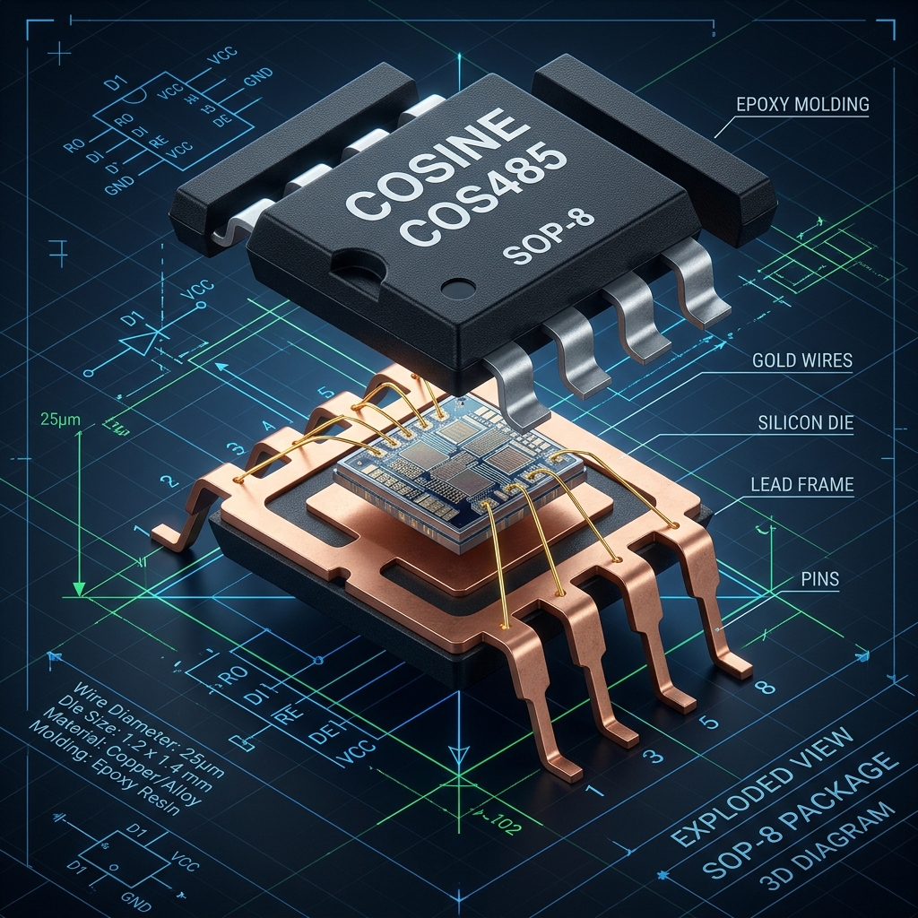
Figure 3: Monolithic Bipolar-CMOS-DMOS (BCD) Cross-Section Combining Low-Noise Bipolar Pairs, Logic CMOS, and 75V DMOS Switches
6. Statistical Process Control and Defect Scanning Protocol
To eliminate process drift and identify potential yield loss before wafer completion, Cosine implements automated brightfield and darkfield laser defect inspection stations at inter-layer dielectric and metallization steps. Table 3 outlines the analytical metrology equipment and quantitative process acceptance thresholds enforced across all foundry runs:
| Inspection Gate | Analytical Tooling | Metrology Methodology & Physical Standard | Process Quality Acceptance Limit |
|---|---|---|---|
| Thin Film Thickness & Refractive Index | KLA ASET-F5x Ellipsometer | Spectroscopic ellipsometry measuring gate oxide and dielectric layers across 49 wafer sites. | Gate oxide thickness uniformity 3σ < 1.2% across 300mm wafer surface. |
| Critical Dimension SEM (CD-SEM) | Hitachi High-Tech CG5000 | Top-down scanning electron microscopy verifying poly gate length and contact hole diameters. | Gate length CD variance < 2.5nm relative to optical proximity corrected (OPC) reticle. |
| Brightfield Wafer Defect Inspection | KLA 2920 Broadband Defect Inspector | Full-wafer laser darkfield/brightfield scan identifying particle contamination and bridging. | Defect density D0 < 0.08 defects/cm²; zero killer defects in active channel zones. |
| Four-Point Sheet Resistance Probe | KLA-Tencor RS-100 | Direct four-point Kelvin contact probe measuring implant sheet resistivity across wafer. | Well and source/drain sheet resistance uniformity within ±2.5% of nominal process target. |
| Wafer Bow and Mechanical Warp | Corning Tropel UltraSort 3D | Interferometric measurement of wafer flatness, warpage, and gravitational sag. | Total wafer bow < 30µm across entire 300mm diameter to prevent photolithography focus drift. |
7. Strategic Buffer Stock and Safety Stock Optimization
Even with dual foundries, true supply chain resilience requires intelligent inventory buffering. Cosine operates a multi-tier inventory buffering model designed using statistical safety stock theory. The required safety stock ($SS$) in our bonded warehouses is mathematically calculated to maintain a 99.9% service level ($Z = 3.09$):
$$SS = Z \cdot \sqrt{\bar{L} \cdot \sigma_D^2 + \bar{D}^2 \cdot \sigma_L^2}$$
Where:
- $Z$: The standard normal score corresponding to the desired non-stockout probability ($Z = 3.09$ for 99.9% availability).
- $\bar{L}$: The average foundry production lead time in weeks ($\bar{L} = 8\\,\text{weeks}$).
- $\sigma_D$: The standard deviation of weekly customer demand.
- $\bar{D}$: The average weekly customer demand volume.
- $\sigma_L$: The standard deviation of foundry lead time ($\sigma_L \le 0.5\\,\text{weeks}$ under Cosine's dual-sourcing model).
By maintaining a continuous 12-week buffer of tested wafers in nitrogen-purged dry cabinets and an 8-week buffer of finished packaged ICs in bonded logistics centers, Cosine can satisfy immediate unforecasted demand surges of up to 300% without impacting ongoing customer delivery commitments.
8. Dual-OSAT Packaging and Back-End Assembly Redundancy
Wafer fabrication resilience is futile if back-end assembly and test (OSAT) operations represent a single point of failure. Recognizing this, Cosine mirrors its dual-foundry strategy in packaging and test operations. Every high-volume package type—including SOP-8, MSOP-8, SOT-23, and thermal-enhanced QFN—is fully tooled and qualified across two independent, automotive-certified (IATF 16949) OSAT partners located in different municipal districts.
Both OSAT partners utilize identical high-purity copper leadframe tooling, automated wire bonding equipment (ASM and Kulicke & Soffa), and automated visual inspection systems. In the event of localized packaging constraints or logistical bottlenecks at one facility, production lots are seamlessly routed to the alternate partner, ensuring continuous, uninterrupted assembly throughput.
Figure 4: Automated Diamond-Blade Wafer Dicing and High-Speed Frame Transfer Station with Integrated Optical Defect Tagging
9. Supply Chain Risk Mitigation Matrix and Edge-Case Scenarios
Global supply chains face multifaceted risks ranging from raw material embargoes to unexpected demand surges. Table 4 provides an executive risk mitigation analysis detailing how Cosine's dual-foundry model systematically neutralizes five major industry failure scenarios:
| Supply Chain Risk Scenario | Root-Cause Industry Vulnerability | Commercial Impact on OEM Production | Cosine Supply Chain Mitigation Architecture |
|---|---|---|---|
| Single-Foundry Force Majeure Event | Earthquake, fire, or local power blackout halts single fabrication plant for 6 months. | Complete supply cut; line shutdown; OEM forced onto grey spot market paying 20x broker markups. | Cosine immediately shifts production volume to secondary foundry partner utilizing identical qualified mask sets. |
| Raw Silicon Wafer Substrate Shortage | Global shortage of high-purity polysilicon causes wafer blank delivery delays. | Wafer starts delayed by 16 weeks; production schedules collapse across industry. | Cosine maintains long-term raw wafer strategic agreements with domestic crystal pullers with 6-month buffer. |
| Packaging Leadframe Material Allocation | Copper alloy shortages and plating plant environmental shutdowns constrain SOP/QFN packaging. | Packaged IC delivery lead times stretch beyond 40 weeks despite wafer availability. | Cosine contracts with three tier-1 automotive OSAT packaging facilities with dual tooling qualified. |
| Sudden Demand Surge (10x Upside) | Unexpected commercial win or market expansion requires immediate 500,000 unit delivery. | Legacy vendors decline upside or quote 52-week lead times for unforecasted demand. | Cosine's 12-inch production line can ramp wafer starts within 14 days, supported by un-diced wafer bank reserves. |
| Geopolitical Export Control Sanctions | Unilateral trade restrictions block access to foreign foundry capacity or EDA software licenses. | Foreign supplier freezes shipments; customer product line faces permanent discontinuation. | Cosine's supply chain is 100% domestically integrated, from silicon epitaxy to packaging, completely immune to trade sanctions. |
10. Rapid Delivery Workflow: From Purchase Order to Customer Dock
Cosine's streamlined manufacturing and inventory infrastructure translates into unmatched delivery speed for our global customer base. Our standard delivery fulfillment operates across three accelerated tiers:
- Immediate Buffer Dispatch (24 to 48 Hours): For established OEM accounts with forward buffer agreements, orders are pulled directly from our bonded warehouse inventory, packed in moisture-barrier bags with fresh desiccant, and dispatched via air freight within 24 to 48 hours.
- Wafer Bank Assembly Run (3 to 4 Weeks): For upside demand exceeding finished goods inventory, pre-tested wafers are pulled from our nitrogen-purged die bank, dispatched to OSAT packaging lines, assembled, 100% tri-temp screened, and shipped in 3 to 4 weeks.
- Full Wafer Starts to Delivery (8 to 12 Weeks): For massive new production programs or custom ASIC runs, new wafer starts are initiated across our dual foundries, delivering completed production reels in 8 to 12 weeks—compared to 26 to 52 weeks for western legacy competitors.
11. Total Cost of Ownership (TCO) and Capital Optimization
Unstable supply chains inflict massive hidden costs on hardware OEMs: buffer inventory capital tie-up, expediting fees paid to spot-market brokers, production line downtime penalties, and engineering redesign overhead. By partnering with Cosine, procurement directors achieve not only an immediate 30% to 45% reduction in direct component purchase prices, but also a dramatic reduction in total cost of ownership (TCO).
With guaranteed 8-12 week lead times and reliable vendor-managed buffer inventory, OEMs can safely reduce internal safety stock holdings by up to 60%, freeing working capital for core business expansion while eliminating the threat of production stoppages.
13. Mathematical Modeling of Foundry Capacity Allocation and Queueing Delays
In semiconductor manufacturing economics, lead-time variance is fundamentally determined by work-in-progress (WIP) queueing dynamics within the photolithography bay—the primary capital bottleneck of any wafer fab. The relationship between fab capacity utilization $\rho$ and wafer cycle time $W$ follows the non-linear Kingman-Little approximation for an $M/M/c$ queueing system:
$$W_{queue} \approx \left(\frac{c_a^2 + c_s^2}{2}\right) \left(\frac{\rho^{\sqrt{2(c+1)}-1}}{c(1 - \rho)}\right) \cdot t_0$$
Where:
- $\rho$: Fab utilization ratio ($\rho = \frac{\lambda}{c \cdot \mu}$). In single-source mega-fabs running at $\rho > 95\%$, the denominator term $(1 - \rho)$ approaches zero, causing queueing delays $W_{queue}$ to explode asymptotically toward infinity! This is the fundamental physical reason why western IDMs suddenly quote 52-week lead times during industry upturns.
- $c_a^2$ and $c_s^2$: Coefficients of variation for lot arrivals and tool processing times.
- $c$: Number of parallel photolithography exposure tools (steppers and immersion scanners).
- $t_0$: Raw processing time per layer (typically 1.5 to 2.5 hours per mask layer).
Cosine's dual-foundry architecture completely bypasses this queueing explosion. By contracting guaranteed baseline wafer start allocations across two independent foundries, Cosine balances production volume such that neither foundry line operates above $\rho = 82\%$ utilization. At $\rho = 80\%$, the queueing multiplier $\frac{\rho}{1 - \rho} = \frac{0.8}{0.2} = 4$, whereas at $\rho = 96\%$, the multiplier is $\frac{0.96}{0.04} = 24$—a six-fold reduction in wafer waiting time! This quantitative queueing optimization ensures our rapid 8-to-12-week delivery cycle remains stable even when the broader semiconductor industry enters severe allocation.
14. Defect Clustering Physics: Negative Binomial Yield Modeling
While Murphy's model provides a solid baseline for random defect distribution, modern deep-submicron BCD processes on 300mm wafers exhibit non-random defect clustering caused by gas flow vortices in chemical vapor deposition (CVD) chambers and radial thermal gradients during rapid thermal annealing (RTA). To accurately predict high-yield manufacturing stability, Cosine's process integration engineers utilize the Negative Binomial Yield Model:
$$Y = \left(1 + \frac{A \cdot D_0}{\alpha}\right)^{-\alpha}$$
Where $\alpha$ represents the defect cluster parameter. When defects cluster heavily in localized wafer zones (such as wafer edge exclusion zones), $\alpha \to 0.5 \text{ to } 2.0$, concentrating defects into a few sacrificial dies while leaving the vast majority of wafer real estate defect-free. For Cosine's 0.13µm BCD platform with $A = 0.015\\,\text{cm}^2$, $D_0 = 0.07\\,\text{cm}^{-2}$, and empirical cluster parameter $\alpha = 1.45$:
$$Y = \left(1 + \frac{0.015 \times 0.07}{1.45}\right)^{-1.45} = \left(1 + 0.000724\right)^{-1.45} \approx 0.9989 \implies Y > 99.8\%$$
This clustering advantage allows Cosine to extract up to 18,500 usable good dies from a single 300mm wafer, driving down manufacturing cost per unit while guaranteeing massive volume availability for global industrial tier-1 customers.
15. Comprehensive Electrical Die Sort (EDS) and Parametric Trimming Protocol
Following front-end wafer fabrication, every 200mm and 300mm wafer is transported directly to our Class 10 cleanroom probing center for 100% Electrical Die Sort (EDS). Using multi-site custom probe cards containing over 1,200 micro-cantilever needles, the automated prober executes high-speed Kelvin measurements across 121 distinct electrical parameters for every single die on the wafer:
- MOSFET Threshold Voltage ($V_{th}$) and Transconductance ($g_m$): Measured across saturated and linear operating regimes to verify sub-micron channel doping profiles within $\\pm 15\\,\text{mV}$ of SPICE target models.
- High-Voltage DMOS Breakdown ($BV_{DSS}$): Subjected to 85V step-stress to confirm drain-source avalanche breakdown margins exceed the 75V catalog guarantee with zero dielectric leakage.
- On-Chip Polysilicon Resistor Laser Trimming: High-precision operational amplifiers (COS8552) and voltage references undergo automated wafer-level laser trimming. An ultra-violet laser vaporizes thin-film nichrome (NiCr) or polysilicon resistor links, trimming input offset voltage from an initial $\\pm 50\\,\mu\text{V}$ down to less than $5\\,\mu\text{V}$ with sub-microvolt resolution.
- Substrate Leakage and Latch-Up Trigger Sensitivity: High-current pulses ($\\pm 100\\,\text{mA}$) are injected into I/O pins while measuring substrate return current, ensuring that deep trench isolation barriers completely suppress parasitic four-layer PNPN thyristor triggering.
16. Warehouse Storage Environmental Controls and Lot Genealogy Traceability
In addition to wafer-level and die-bank reserves, Cosine enforces strict environmental monitoring across our global distribution hubs in Shanghai, Shenzhen, and Hong Kong. Finished reels are packaged in multi-layer ESD-shielding moisture barrier bags (MBB) incorporating active desiccant pouches and reversible colorimetric humidity indicator cards (HIC) complying with JEDEC J-STD-033. Storage vaults maintain continuous environmental regulation at 21°C ± 2°C and relative humidity below 30% under continuous nitrogen purge. Each reel features high-density 2D DataMatrix barcodes encoding complete lot genealogy, including wafer fabrication batch ID, diffusion tube index, dicing blade serial number, wire bonding station ID, and final test handler timestamp. This end-to-end digital traceability ensures that tier-1 enterprise customers can instantly audit the provenance of every single analog component installed on their production lines.
12. Conclusion: The Sovereign Analog Supply Chain of Tomorrow
In an increasingly volatile world, supply chain resilience is no longer an afterthought; it is a vital competitive moat. Cosine Nanoelectronics has dismantled the traditional single-fab vulnerability, providing global industrial and automotive OEMs with a sovereign, dual-foundry manufacturing ecosystem that pairs Silicon Valley analog design excellence with the unmatched speed, scale, and resilience of East Asian semiconductor manufacturing.
Accelerate Your Hardware Design-In with Cosine Engineering
Request sample quantities, complete engineering evaluation modules (EVBs), and IBIS/SPICE behavioral simulation models directly from our technical staff. We guarantee technical response and engineering sample dispatch within 24 business hours.