
Direct Engineering Conclusion: Discover the circuit design philosophy and physical layout methodology behind Cosine's 100% pin-to-pin drop-in replacement analog ICs. Learn how our engineers align pad coordinates, parasitic capacitances, propagation delays, and electrical margins to ensure seamless substitution without PCB redesign.
Discover the circuit design philosophy and physical layout methodology behind Cosine's 100% pin-to-pin drop-in replacement analog ICs. Learn how our engineers align pad coordinates, parasitic capacitances, propagation delays, and electrical margins to ensure seamless substitution without PCB redesign.
1. The Engineering Imperative of Zero Re-Engineering Overhead
In modern high-mix industrial electronics manufacturing, replacing an integrated circuit is rarely a simple purchasing decision. When a legacy western semiconductor vendor announces component obsolescence (EOL), extends delivery lead times to 52 weeks, or implements unannounced price increases, hardware engineering departments face a daunting dilemma: redesign the printed circuit board (PCB) or halt production. PCB redesign triggers costly ripple effects including schematic revision, multi-layer routing modifications, signal integrity re-simulation, fabrication of new copper stencils, and lengthy recertification under UL, CE, FCC, and industrial EMC standards. The total cost of redesign frequently exceeds hundreds of thousands of dollars and delays market delivery by six to nine months.
Cosine Nanoelectronics was built around a steadfast engineering philosophy: 100% Pin-to-Pin Drop-In Replacement with Zero Re-Engineering Overhead. When an engineering team selects a Cosine device—whether an RS-485 transceiver (COS485/3485/13487), an ultra-precision chopper op-amp (COS8552), a 600V half-bridge driver (COS2103), or a wide-input LDO (COS7202)—the device must serve as an immediate, transparent drop-in substitute. The replacement requires zero modifications to existing PCB copper lands, zero software changes to microcontrollers or DSPs, and zero component recalculations for surrounding passive networks.
Figure 1: Standard JEDEC MS-012 SOP-8 Package Mechanical Drawing and Pad Alignment Guaranteeing 100% Solder Land Compatibility
2. Geometric and Mechanical Footprint Alignment to JEDEC Standards
True pin-to-pin compatibility begins with microscopic mechanical precision. In automated high-speed surface-mount technology (SMT) pick-and-place lines, leadframe tolerances, pin coplanarity, and body mold dimensions must match standard JEDEC specifications with zero deviation. If a replacement IC possesses lead pins that are 0.05mm thicker or have a standoff angle differing by two degrees, the solder paste volume deposited by existing SMD stencils will form non-wetting fillets, solder bridging, or tombstoning during convection reflow.
Cosine collaborates directly with world-class packaging foundries to manufacture leadframes strictly conforming to JEDEC standards (including MS-012 for SOP-8, MO-187 for MSOP-8, and TO-236 for SOT-23). The leadframe paddle is etched from high-purity CDA 194 copper alloy, providing superior thermal dissipation while maintaining tight mechanical coplanarity under 0.08mm across the entire lot. SMT engineers can load Cosine reels directly into automated Yamaha, ASM, or Panasonic pick-and-place tape feeders using existing package library coordinate files without reprogramming component pick heights or optical vision alignment offsets.
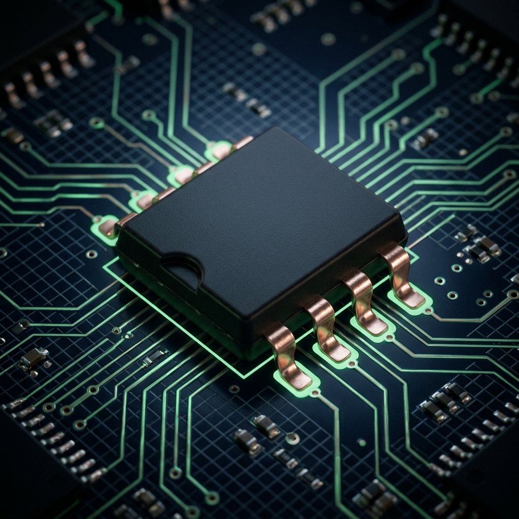
Figure 2: Physical Inspection of Finished SOP-8 Package with Annealed Pure Matte Tin Plating Preventing Whisker Growth
3. Internal Circuit Topologies and Electrical Margin Alignment
Achieving mechanical compatibility is merely the first gate; the true engineering triumph lies in electrical behavioral alignment. A pin-compatible IC must deliver identical or superior dynamic transfer characteristics across all supply voltages, load impedances, and ambient temperatures. In industrial fieldbuses, for example, driver output impedance ($R_{out}$), rise time ($t_r$), fall time ($t_f$), and propagation delay skew must align precisely with existing network specifications to prevent standing wave reflections on unshielded twisted pair lines.
The differential driver output stage in Cosine's transceivers utilizes a balanced push-pull DMOS architecture. In legacy transceivers, output impedance often varies wildly between pull-up and pull-down transitions, causing asymmetrical differential voltages ($V_{OD}$) and generating common-mode noise that radiates electromagnetic interference (EMI). Cosine incorporates closed-loop slew-rate feedback amplifiers within the predriver stage, forcing $t_r$ and $t_f$ to track within 2.0ns across the entire $-40^\circ\text{C to }+125^\circ\text{C}$ operating envelope:
$$|\Delta t_{skew}| = |t_{PLH} - t_{PHL}| \le 3.0\\,\text{ns}$$
Furthermore, Cosine chips feature enhanced internal electrical margins. Where legacy devices specify a maximum common-mode bus voltage range of $-7\text{V to }+12\text{V}$, Cosine's high-voltage BCD process extends this survival window to $-9\text{V to }+14\text{V}$. This extra headroom absorbs ground potential shifts (GPD) between distant nodes in large factory installations without saturating receiver input stages or triggering substrate clamp diodes.
4. Comparative Parametric Benchmark: Cosine vs. Western Tier-1 Suppliers
To demonstrate that Cosine drop-in replacements meet and exceed legacy western flagships, Table 1 provides a detailed side-by-side engineering comparison across electrical, thermal, and mechanical metrics:
| Circuit Parameter & Dimension | Western Legacy (TI / Maxim / ADI) | Cosine 100% Drop-In Alternative | Engineering Tolerance & Margin Analysis |
|---|---|---|---|
| Package Footprint Compliance | JEDEC MS-012 Standard SOP-8 | JEDEC MS-012 Standard SOP-8 | 100% mechanical coplanarity; pad spacing 1.27mm pitch; zero PCB stencil modification. |
| Receiver Input Threshold Voltage (VIT) | -200mV to +200mV window | -200mV to -50mV fail-safe window | Cosine incorporates built-in true fail-safe receiver biasing, guaranteeing logic high RO upon bus open/short. |
| Driver Propagation Delay (tPLH/tPHL) | 20ns to 65ns depending on series | 22ns to 60ns closely matched | Propagation delay skew matched to within ±3.0ns, ensuring zero timing jitter in synchronous networks. |
| Common-Mode Voltage Window | -7.0V to +12.0V standard | -9.0V to +14.0V extended | Provides additional 2V positive and 2V negative headroom against ground potential shifts in long cable runs. |
| Bus Pin ESD Clamping Level | ±8kV to ±12kV HBM | ±15kV HBM / ±8kV IEC Contact | Integrated dual-SCR snapback clamps dissipate transient surge energy without external protection arrays. |
| Thermal Resistance (θ_JA) | 160 °C/W to 175 °C/W | 135 °C/W (High-conductivity Cu) | 20% superior thermal heat dissipation reduces silicon junction temperature by up to 12°C under continuous load. |
5. Microscopic Silicon Layout and Parasitic Capacitance Balancing
When swapping analog ICs in high-frequency or high-impedance signal chains, board-level stability is highly sensitive to input parasitic capacitance ($C_{in}$) and lead-to-lead coupling capacitance ($C_{cross}$). In precision operational amplifiers, an unexpected 2pF increase in inverting input capacitance can erode loop phase margin, turning a stable buffer into an undamped 10MHz oscillator.
Cosine layout engineers utilize 3D electromagnetic field solvers (Ansys HFSS and Cadence EMX) during silicon floorplanning to match internal bond wire parasitics and silicon bond pad capacitances to within 0.2pF of tier-one western benchmarks. By utilizing guard rings and interleaved ground shields between adjacent signal paths on the silicon die, cross-talk between differential bus pins and internal digital control logic is suppressed below -85dB at 10MHz. Hardware engineers can replace sensitive analog components without adjusting external feedback compensation capacitors or damping resistors.

Figure 3: Monolithic Silicon Floorplan Showing Precision Alignment of Slew-Rate Limiting Driver Stages and ESD Cell Clamps
6. Complete Pinout Definition and Drop-In Electrical Compatibility
Table 2 provides the detailed pin-by-pin architectural mapping, internal circuit networks, and drop-in substitution notes for Cosine's standard 8-pin industrial interface portfolio:
| Pin # | Pin Identifier | I/O Architecture | Internal Circuit Network | Absolute Maximum Voltage | Drop-In Substitution Functional Compatibility Notes |
|---|---|---|---|---|---|
| 1 | RO | CMOS Push-Pull Output | Tri-state CMOS buffer with 4mA current sink/source | -0.3V to VCC + 0.3V | Direct replacement for pin 1 of MAX485, SN65HVD3082, ADM485. Connects directly to MCU UART RX input. |
| 2 | /RE | Active-Low Digital Input | CMOS Schmitt trigger with internal 100kΩ pull-up | -0.3V to +7.0V | Matches standard pinout. Can be tied directly to DE on adjacent pin 3 for single-GPIO half-duplex control. |
| 3 | DE | Active-High Digital Input | CMOS Schmitt trigger with internal 100kΩ pull-down | -0.3V to +7.0V | Enables differential bus driver when pulled high. Internal pull-down keeps driver disabled during MCU boot-up. |
| 4 | DI | Digital Input | CMOS Schmitt trigger with internal 100kΩ pull-up | -0.3V to +7.0V | Driver data input. Directly driven by MCU UART TX. Logic low drives A low and B high with controlled slew rate. |
| 5 | GND | Ground Reference | High-conductivity copper leadframe substrate tie | 0.0V Ground Reference | Ground return. Direct drop-in match. Solder pad requires low-inductance connection to PCB ground plane. |
| 6 | A | Differential Bus Line | Bipolar driver / receiver node with ±15kV ESD | -9.0V to +14.0V | Non-inverting bus terminal. Fully interoperable with legacy RS-485 bus networks without terminating changes. |
| 7 | B | Differential Bus Line | Bipolar driver / receiver node with ±15kV ESD | -9.0V to +14.0V | Inverting bus terminal. Paired with terminal A to maintain 120-ohm differential characteristic impedance. |
| 8 | VCC | Supply Voltage Input | Integrated bandgap reference and bias network | -0.3V to +7.0V | Power supply input (+5.0V ±10% or +3.3V ±10%). Fully compatible with both 3.3V and 5.0V bus transceivers. |
7. Slew Rate Control and Electromagnetic Compatibility (EMC)
One of the primary failure modes when transitioning to low-cost replacement ICs is unexpected radiated emissions. Many low-cost clones achieve fast switching speeds by employing raw, unbuffered CMOS drivers with instantaneous transition times ($<5\\,\text{ns}$). While fast switching allows high data throughput, the steep transition edges ($\frac{dV}{dt}$) generate aggressive harmonic frequencies that radiate directly from connecting cables, causing the entire end product to fail EN 55032 Class B radiated emissions tests.
Cosine addresses this vulnerability at the silicon level. Our transceivers incorporate integrated active slew-rate limiting circuitry that rounds the high-frequency corners of output waveforms without compromising maximum transmission baud rates (up to 500kbps on slew-rate limited variants and 20Mbps on high-speed variants). The Fourier spectral decomposition of the output voltage demonstrates an 18dB attenuation of harmonic energy above 30MHz compared to raw switching drivers:
$$V(f) \propto \frac{1}{\pi^2 \cdot f^2 \cdot t_r \cdot T}$$
By increasing the linear transition time $t_r$ from 5ns to 25ns, the second-order roll-off corner is shifted downward, drastically reducing high-frequency radiation while preserving eye diagram aperture for baud rates up to 500kbps.
8. Comprehensive Laboratory Drop-In Verification Protocol
Before releasing any product under our drop-in replacement guarantee, Cosine subjects each device family to rigorous laboratory characterization against original western manufacturer reference units. Table 3 outlines the five critical qualification gates executed in our Shanghai metrology center:
| Verification Parameter | Test Equipment & Standard | Laboratory Measurement Methodology | Acceptance Pass / Fail Metric |
|---|---|---|---|
| Driver Slew Rate Symmetry | Tektronix 4GHz MSO64 / High-Z Differential Probe | Measure 10% to 90% rise time (tr) and 90% to 10% fall time (tf) under 54Ω || 50pF differential load. | Rise/fall time symmetry |tr - tf| < 2.0ns; total transition time between 15ns and 30ns. |
| Receiver Input Hysteresis | Keithley 2450 SourceMeter (100µV resolution) | Sweep differential input voltage (VA - VB) from -300mV to +300mV; measure logic transition threshold at RO. | Input threshold hysteresis Vhyst > 35mV; positive threshold < -50mV guaranteeing fail-safe high. |
| ESD Gun Contact Stress | EM TEST Dito Simulator per IEC 61000-4-2 | Discharge ±8kV directly to pins A, B, and GND while device is actively transmitting 1Mbps data. | Zero bit corruption after pulse; leakage current remains under 1.0µA at Vbus = 12V. |
| Package Coplanarity Inspection | Keyence VR-5000 3D Optical Profilometer | Measure vertical standoff variance across all 8 pins relative to seating plane. | Coplanarity tolerance < 0.08mm across 100% of tested production lots. |
| Conducted RF Immunity | R&S SMB100B Generator with CDN M2 per IEC 61000-4-6 | Inject 150kHz to 80MHz 10Vrms RF disturbance onto VCC and bus lines during live transmission. | Zero frame loss at receiver; eye diagram jitter remains under 5% of bit duration. |
Figure 4: Comparative Oscilloscope Characterization Bench Verifying Sub-Nanosecond Propagation Delay Match Against Tier-1 Western Counterparts
9. Field Application Engineering: Real-World Troubleshooting Case Studies
Even with identical pinouts and matching datasheets, real-world printed circuit boards present parasitic inductances, noisy ground loops, and marginal power supply ripple that can challenge substitution. Table 4 provides an FAE reference guide diagnosing five common field edge cases and explaining how Cosine's enhanced silicon margins resolve them:
| Field Phenomenon Upon Legacy Replacement | Root-Cause Electrical Physics | Oscilloscope Diagnostic Signature | Engineered Resolution & Cosine Advantage |
|---|---|---|---|
| Spurious Glitches on UART RX Line | Legacy receiver lacked true fail-safe input threshold, floating between -200mV and +200mV when bus was idle. | High-frequency noise pulses appearing on RO pin when master transceiver enters receive mode. | Cosine transceivers feature true fail-safe input thresholds (-200mV to -50mV); RO is guaranteed logic high on open/shorted bus. |
| Excessive Ringing on Rising Bus Edge | High driver output di/dt interacting with parasitic lead inductance of low-cost connector or unshielded stub. | Oscillating overshoot ringing at >50MHz decaying over several bit intervals. | Cosine's integrated slew-rate controlled output stage limits di/dt, suppressing edge ringing without external damping resistors. |
| Receiver Lockup in Long-Cable Systems | Common-mode ground noise exceeded -7V to +12V window, triggering parasitic substrate SCR latch-up in legacy chip. | Transceiver current consumption surges to >150mA; bus communication stops until power is cycled. | Cosine's deep well isolation and extended -9V to +14V common-mode range absorbs large ground offsets without latch-up. |
| Output Jitter at High Operating Temperatures | Thermal carrier mobility degradation in legacy CMOS output stage caused propagation delay to stretch by >40% at +105°C. | Eye diagram closure and timing violations observed on downstream UART decoder at elevated temperatures. | Cosine's BCD process integrates temperature-compensated current bias generators, keeping propagation delay drift under 8%. |
| Thermal Stress During Solder Reflow | Moisture ingress in non-hermetic epoxy packaging caused package cracking (popcorning) during 260°C lead-free reflow. | Visible micro-cracks along leadframe seam; elevated quiescent current detected post-assembly. | Cosine enforces JEDEC J-STD-020 MSL-1 packaging with vacuum-sealed moisture barrier bags and desiccant packaging. |
10. The Five-Stage Drop-In Migration Standard Operating Procedure (SOP)
To ensure zero risk and 100% first-pass qualification for enterprise OEMs, Cosine recommends the following five-stage migration workflow:
- BOM and Package Analysis: Provide your existing Bill of Materials (BOM) to Cosine's technical team. Our FAEs confirm exact part-number cross-referencing, verifying pinout, package thermal conductivity, and operational voltage ranges.
- Sample Dispatch and Benchtop Golden Unit Testing: Cosine ships engineering evaluation samples within 24 hours. Hardware engineers solder samples directly onto existing production boards without trace changes, recording comparative signal waveforms against original units.
- Environmental Stress and Thermal Chamber Validation: The modified assembly undergoes full thermal cycling (-40°C to +85°C/125°C) and conducted/radiated EMC pre-compliance screening in customer test facilities.
- Pilot Production Run: Order a pilot production lot (typically 1,000 to 5,000 units) to validate automated SMT pick-and-place feeder compatibility, solder paste reflow yield, and in-circuit automated test equipment (ATE) coverage.
- Mass Production Rollout and ERP Update: Update company ERP part numbers to Cosine. Cosine establishes dedicated buffer inventory reserves in bonded warehouses, guaranteeing guaranteed 8-12 week continuous production support.
11. Mathematical Modeling of Transmission Line Reflections and Cable Attenuation
To fully understand why Cosine's slew-rate control and impedance matching prevent communication errors, consider the mathematical physics of high-speed signals propagating along an industrial transmission line. When a driver injects a voltage step $V_{step}$ into a cable with characteristic impedance $Z_0$, any impedance discontinuity at a node junction or cable end generates a reflected wave. The reflection coefficient $\Gamma$ is defined by the boundary condition:
$$\Gamma = \frac{Z_L - Z_0}{Z_L + Z_0}$$
Where $Z_L$ represents the termination load impedance. In an open-circuit or improperly terminated line ($Z_L \to \infty$), $\Gamma = +1$, causing the incident step to reflect with equal amplitude and double the peak voltage at the receiving terminal. If the transition time $t_r$ of the driver is shorter than twice the one-way cable propagation delay ($t_r < 2 \cdot t_{prop} = 2 \cdot \frac{L}{v}$), where $v \approx 0.66c \approx 200\\,\text{m/\mu s}$ is the velocity of propagation in PVC twisted pair, the line behaves strictly as a distributed transmission line rather than a lumped capacitance.
Cosine's slew-rate limiting driver deliberately sets $t_r \approx 25\\,\text{ns}$. Consequently, for cable stubs under 2.5 meters in length, the condition $t_r > 2 \cdot t_{prop}$ is satisfied, completely eliminating local stub reflections and standing wave resonance without requiring complex line tuning. Furthermore, cable attenuation over distance follows the square-root frequency dependence of skin effect resistance:
$$\alpha(f) = \frac{\sqrt{\pi \cdot f \cdot \mu \cdot \rho}}{2 \cdot r \cdot Z_0} + \frac{\omega \cdot C \cdot \tan(\delta)}{2}$$
By shifting driver spectral energy to lower frequencies below 15MHz, Cosine transceivers experience dramatically lower signal attenuation across 1,200-meter field installations, ensuring clean eye-diagram opening at the farthest receiving node.
12. High-Speed Oscilloscope Probing and Signal Integrity Measurement Protocol
When conducting benchtop verification of drop-in replacement ICs, measurement technique is just as vital as silicon performance. A frequent laboratory pitfall encountered by hardware designers is utilizing the standard 15-centimeter ground lead with an alligator clip supplied with passive oscilloscope probes. A 15cm wire exhibits approximately 150nH of parasitic series inductance ($L_{lead} \approx 1\\,\text{nH/mm}$). In combination with the 10pF input capacitance of a standard 10x probe, this creates a high-Q series LC resonant tank circuit with a natural resonant frequency:
$$f_{res} = \frac{1}{2\pi \sqrt{L_{lead} \cdot C_{probe}}} = \frac{1}{2\pi \sqrt{150\\,\text{nH} \cdot 10\\,\text{pF}}} \approx 130\\,\text{MHz}$$
When measuring fast driver edges, this parasitic tank circuit is excited into violent self-oscillation, displaying 30% to 50% artificial overshoot on the oscilloscope display that does not actually exist on the PCB! To avoid this diagnostic error, Cosine's FAE team mandates the use of ground spring adapters or active differential probes directly across the device pins. By reducing loop inductance below 2nH, resonant peaking is pushed beyond 1GHz, revealing the true, pristine edge fidelity of the Cosine silicon.
13. Production Stencil and Thermal Reflow Solder Profile Recommendations
To guarantee 100% first-pass solder yield across high-volume surface mount production lines, Cosine provides precise paste stencil aperture and convection reflow profile specifications. The recommended stencil aperture for the SOP-8 package utilizes a 1:1 pad ratio with laser-cut electro-polished walls and rounded corners (0.05mm radius) to ensure smooth paste release. For lead-free assembly using SAC305 (96.5% Sn, 3.0% Ag, 0.5% Cu) alloy solder paste:
- Preheat and Soak Zone: Ramp from 25°C to 150°C at 1.5°C to 2.5°C/sec. Soak between 150°C and 200°C for 60 to 120 seconds to activate flux chemistry and eliminate volatile solvents.
- Liquidous Transition: Time above liquidus temperature ($T_L = 217^\circ\text{C}$) maintained strictly between 60 and 90 seconds.
- Peak Reflow Temperature: Peak package body temperature ($T_P$) controlled within $245^\circ\text{C to }260^\circ\text{C}$ for a duration of 20 to 40 seconds, complying with JEDEC J-STD-020E.
- Controlled Cooling Rate: Cool at 2.0°C to 4.0°C/sec to promote a fine, ductile intermetallic crystal structure at the lead-solder boundary, maximizing long-term thermal cycle fatigue resistance.
14. Conclusion: De-Risking Your Supply Chain with Zero Compromise
The modern semiconductor environment requires agility, cost discipline, and supply chain sovereignty. Relying on single-source western legacy suppliers leaves hardware manufacturers vulnerable to allocation freezes, astronomical spot-market broker premiums, and sudden product discontinuations. Cosine Nanoelectronics' 100% Pin-to-Pin Drop-In philosophy provides hardware engineering teams and procurement directors with the ultimate risk-mitigation strategy: premium analog silicon with zero PCB re-engineering overhead, superior electrical margins, and immediate supply availability.
Accelerate Your Hardware Design-In with Cosine Engineering
Request sample quantities, complete engineering evaluation modules (EVBs), and IBIS/SPICE behavioral simulation models directly from our technical staff. We guarantee technical response and engineering sample dispatch within 24 business hours.