
COS13487EESA Half-Duplex RS-485/RS-422 Transceiver
⚡ Executive Engineering Sourcing Summary (BLUF): COS13487 is an industrial-grade interface ic in standard SOP-8 packaging operating across 4.5V to 5.5V with 500 kbps and ±15kV HBM ESD. It provides verified 100% pin-compatible drop-in replacement for MAX13487EESA+T, THVD1406DR, eliminating board redesign while delivering ISO 9001 quality assurance, -40°C to +125°C extended temperature operation, and guaranteed 4-to-6-week production delivery.
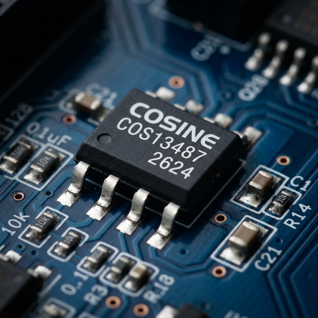
Key Electrical Parameter Matrix
Absolute Maximum Ratings & Operating Boundaries
Stresses beyond these limits may cause permanent damage. Exposure to absolute maximum rated conditions for extended periods may affect device reliability.
Architectural Innovations & Silicon Advantages
COS13487EESA Half-Duplex RS-485/RS-422 Transceiver utilizes an advanced 0.18µm BCD analog mixed-signal process. An integrated hardware state machine automatically monitors data transmission, eliminating external direction control GPIO pins and optical isolators. On-chip dual-stage clamping networks deliver ±15kV human-body model ESD resilience, safeguarding sensitive microcontrollers from industrial line surges without requiring bulky external TVS diodes.
EDA CAD Models & Symbols (Design-In Kit)
Pre-verified schematic symbols, PCB footprints, and 3D STEP models for rapid board turnarounds.
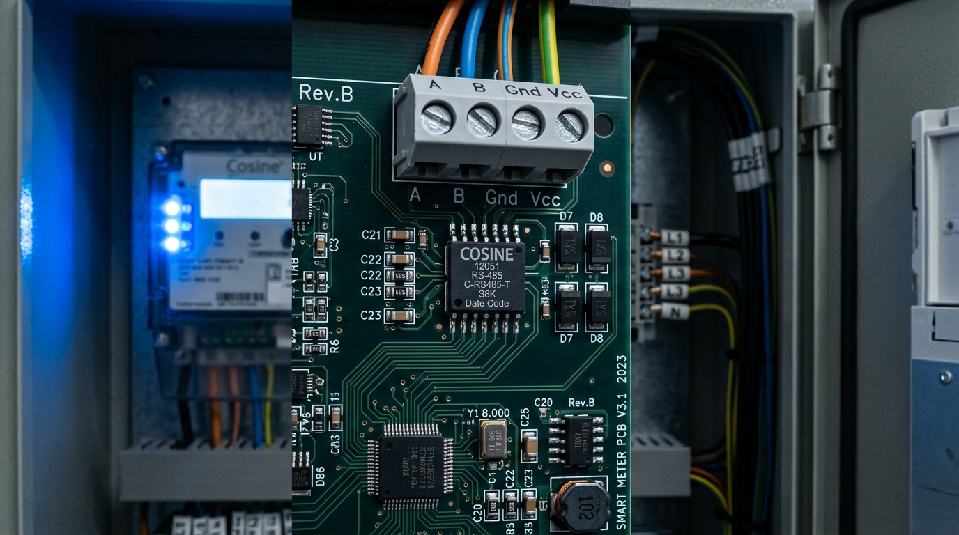
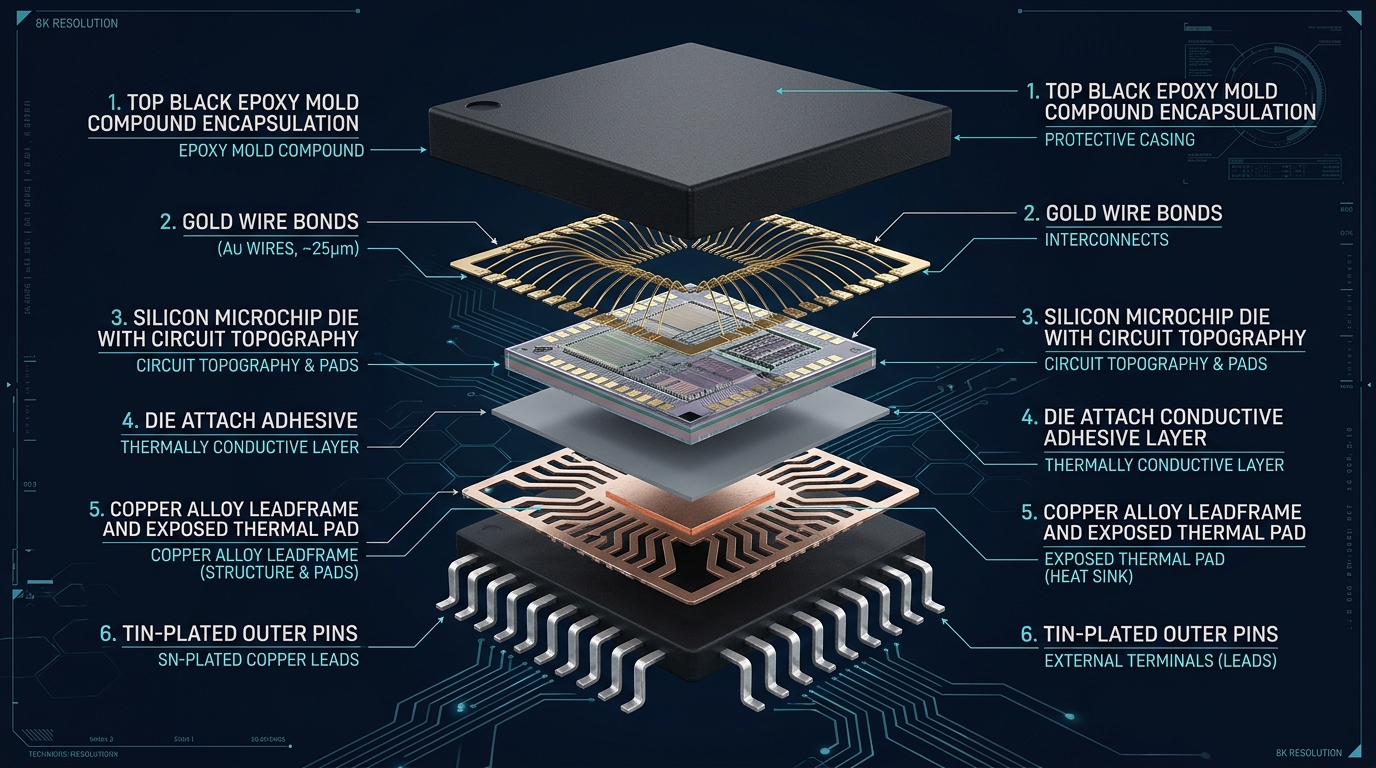
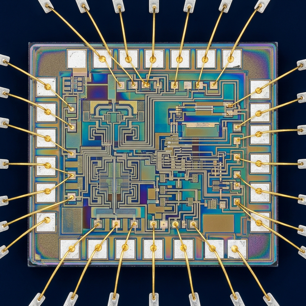
Visual Engineering Gallery: Application Scene & Exploded Views
Inspecting the physical deployment environment, internal silicon micro-architecture, and package construction of COS13487.
1:1 Drop-In Competitor Cross-Reference Matrix
Direct pin-compatible alternatives to simplify procurement and eliminate single-source risks.
| Competitor Part Number | Manufacturer | Compatibility Type | Engineering Benefit of Cosine COS13487 |
|---|---|---|---|
| MAX13487EESA+T | Maxim / ADI | 100% Pin-to-Pin Drop-In | Identical auto-direction, +15kV ESD, wider supply range |
| THVD1406DR | Texas Instruments | Functional & Pin Compatible | Higher EFT transient immunity, reduced quiescent current |
SOP-8 Pin Configuration & Functional Descriptions
| Pin # | Pin Name | Type | Functional Description & PCB Routing Notes |
|---|---|---|---|
| 1 | RO | Output | Receiver Output. When active, high if A-B > -50mV, low if A-B < -200mV. |
| 2 | /RE | Input | Receiver Enable. Active LOW. Connect to GND for continuous receive. |
| 3 | DE | Input | Driver Enable. Tied internally to Auto-Direction state machine logic. |
| 4 | DI | Input | Driver Input. Low level automatically activates the driver output. |
| 5 | GND | Power | Ground reference (0V). |
| 6 | A | I/O Bus | Non-inverting RS-485 receiver input and driver output. |
| 7 | B | I/O Bus | Inverting RS-485 receiver input and driver output. |
| 8 | VCC | Power | Positive power supply input (+3.0V to +5.5V). Bypass with 0.1uF. |
Hardware Engineer Design-In & PCB Layout Checklist
- Bypass Capacitors: Place a 100nF low-ESR ceramic capacitor directly adjacent to the power supply pins and return ground plane within 2mm trace distance.
- Signal Routing: Keep high-speed or differential signal traces short, symmetrical, and avoid routing over split ground planes.
- Thermal Management: For high-current or power packages, connect exposed thermal ground pads to multiple copper thermal vias into inner ground layers.
- ESD Protection: While COS13487 incorporates on-chip ±15kV HBM ESD protection, optional external bidirectional TVS diodes can be added for harsh field cable terminals.
Orderable Part Numbers & Packing Specifications
| Orderable Part Number | Package | Carrier / Packing | Standard Reel MOQ | Sample Lead Time |
|---|---|---|---|---|
| COS13487 | SOP-8 | Tape & Reel (13" Embossed Carrier) | 2,500 / 3,000 pcs | 24h Express Courier |
Request Free Sample Kit for COS13487
Need evaluation chips, reference schematics, or pin-compatibility confirmation? Our senior application engineering team dispatches samples worldwide within 24 hours.