
Green Semiconductor Supply Chains
Designing eco-friendly, energy-efficient integrated circuits and enforcing lead-free material control.
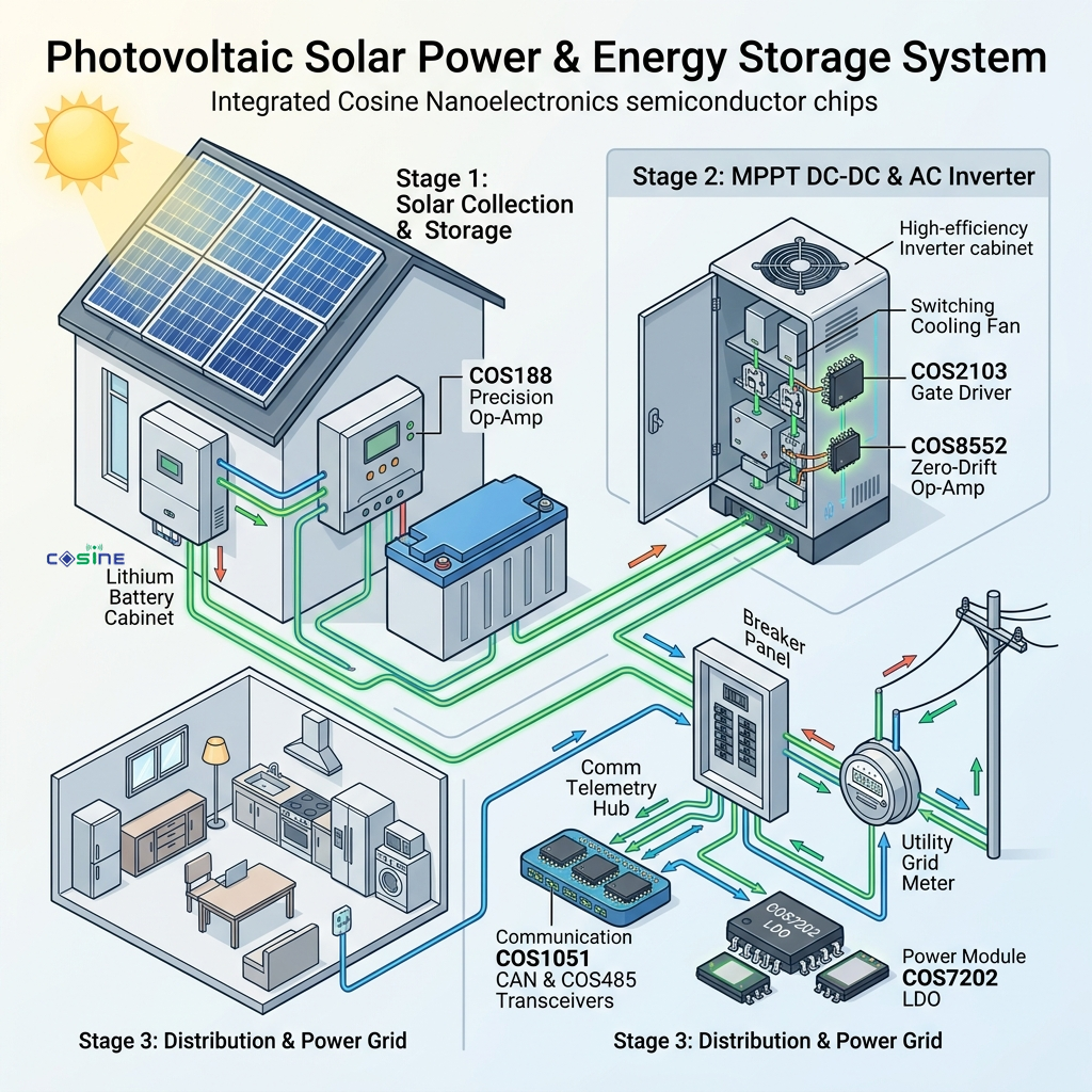
Our ESG Commitments & Clean Energy
As a modern fabless semiconductor designer, we evaluate the environmental impact of both our chip designs and upstream manufacturing foundries. We prioritize foundries and assembly partners (TSMC, SMIC, ASE, JCET) that employ active green grid integrations, wastewater recycling, and rooftop solar arrays to reduce Scope 2 and 3 carbon footprints.
In our chip designs, we optimize power management circuits to operate with minimal standby currents. For instance, our low-dropout regulator **COS7202** consumes a mere 15μA of quiescent current, ensuring battery-operated smart water meters and gas sensors last for over 10 years without replacement, directly cutting e-waste.
Upstream Circularity: Over 90% of cooling water at our partner wafer fabrication foundries is recycled through reverse osmosis (RO) circular loops, minimizing direct freshwater usage.
Four Pillars of Cosine Green Electronics
Providing certified, high-performance green chips for global B2B procurement channels.
RoHS & REACH Compliance
We certify that all microchips are free from hazardous elements, fully satisfying European Union Directive 2011/65/EU and REACH SVHC declarations.
Lead-Free Lead Frames
By using 100% pure matte tin (Sn) electroplating over copper frames, we eliminate lead (Pb) elements, ensuring compatibility with lead-free reflow SMT profiles.
Ultra-Low Quiescent Current
We develop high-efficiency LDO and amplifier topologies that cut static current consumption, extending portable battery runtime and lowering heat waste.
Halogen-Free Molding
Our plastic encapsulation uses halogen-free epoxy molding compounds, which prevent the emission of toxic halogen gases in case of thermal incidents.